
VIA Part 4 – A Deep Dive into Centaur’s Last CPU Core: CNS


The x86-64 instruction set powers the vast majority of PCs, consoles, and servers. However, the number of x86 licensees has always been small, so it’s important to keep track of the few that are left. While Intel and AMD have been at each other’s throats chasing the performance crown, VIA, the former owner of Centaur, has quietly targeted the lower power laptop and embedded market. We’ve covered a couple of their previous chips, like the VIA Nano and Zhaoxin LuJiaZui. However, VIA haven’t made any attempts to go head to head with Intel or AMD’s top end designs since the cancellation of then newly acquired Cyrix’ Jalapeno core in 1999.
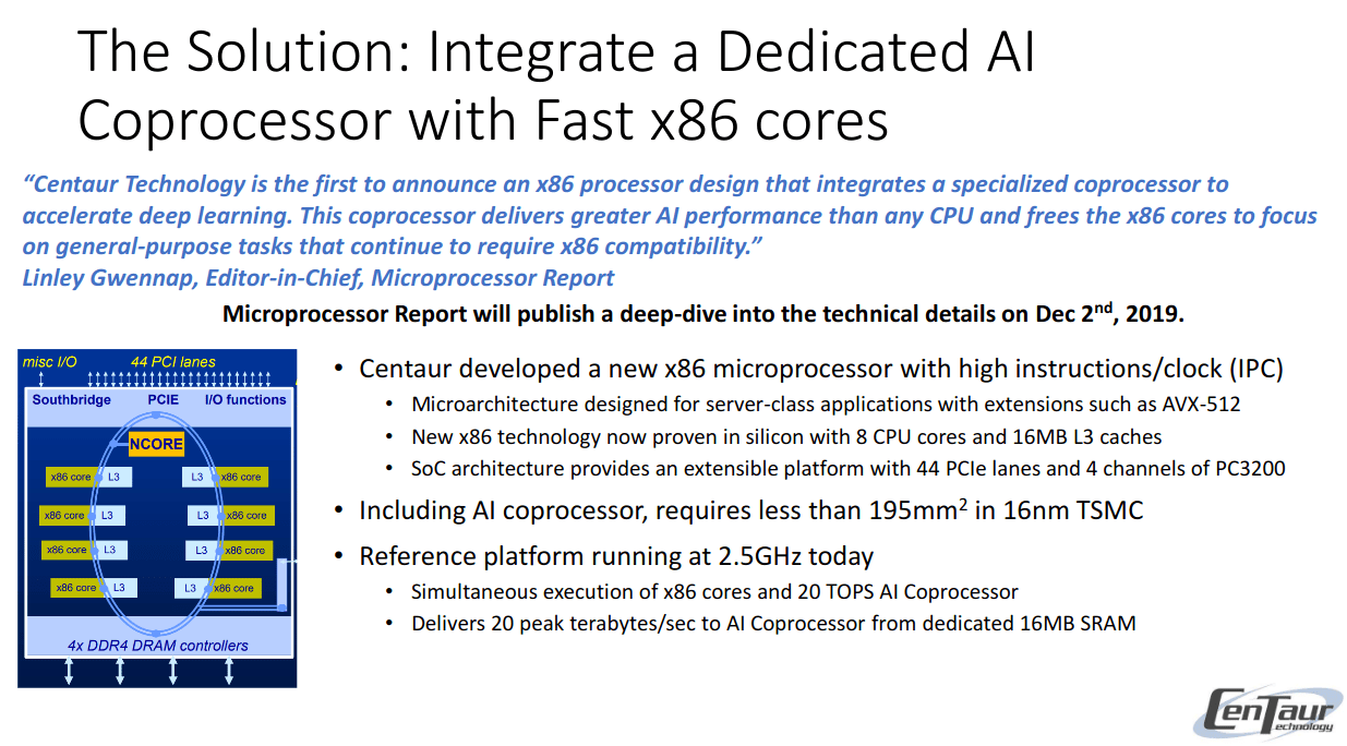
In 2019 things changed and VIA again set their sights on higher performance targets. Following in the footsteps of their now defunct subsidiary Cyrix, the Centaur team announced an x86 core called “CNS”. Unlike Nano, CNS targets server applications and prioritizes high performance with high IPC and AVX-512 support. That puts CNS in a very interesting position. It not only represents a shift away from VIA’s strategy of targeting the low power market, but also stands out as the first non-Intel microarchitecture to implement AVX-512.
But late last year, news broke that Intel was buying the Centaur design house from VIA. This sent shock waves throughout the tech world, because Centaur was the only remaining high performance x86 design house besides Intel and AMD.
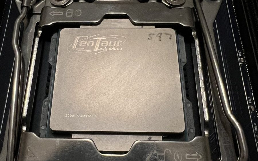
Unfortunately, that most likely killed the CNS effort. However, thanks to Brutus along with our wonderful patreons and supporters, we managed to get one of the few CHA chip samples. In this article, we’re going to take a deep look at the CNS microarchitecture, and see what could have been if it actually released.
Overview and Block Diagram
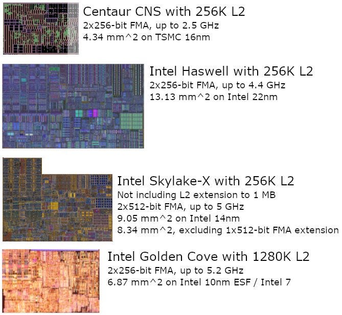
Centaur’s CHA chip comes with eight CNS cores along with a machine learning accelerator, called the NCore. To feed those components, CHA has a 16 MB last level cache, and a quad channel DDR4 memory controller. All of that is implemented on a 194 mm2 die, with TSMC’s 16nm process:
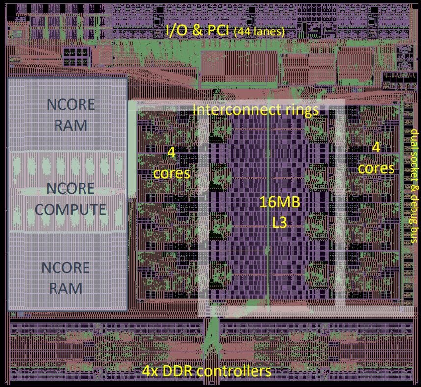
We’re going to focus on the CNS cores, because there were no NCore drivers released publicly or that we could find. Here’s what the architecture looks like from our testing:

Our CNS chip runs at 2.2 GHz, which is impressive for an engineering sample chip when the production chips targeted 2.5 GHz. For testing, it’s set up with quad channel DDR4-3200 memory. For comparison purposes, we ran tests on an Azure NC12 instance. That has a Xeon E5-2690 v3 with SMT disabled, and appears to be running at 3 GHz. However, we’re not sure what kind of memory it has.
Frontend: Branch Prediction Accuracy
Centaur refers to the CNS as “Haswell-Class”
Centaur Adds AI to Server Processor, by Linley Gwennap
Since Centaur says the CNS core is Haswell class, that’s what we’ll compare it with. CNS’s predictor can recognize pretty long patterns, but generally falls short of Haswell’s capabilities. However CNS does appear to have ample storage for branch history. With 512 branches in play, it can keep up excellent prediction accuracy with repeating history lengths up to 24-long. Haswell in contrast falls apart once the pattern length exceeds 16.


CNS’s direction predictor is much more powerful than the one in Nano. Centaur made significant progress since their last attempt at taking on the x86 market. But Intel is a juggernaut with lots of engineering muscle, and they’re not so easy for a small company to catch.
Indirect Branch Prediction
Indirect branches can jump to different places, and add another layer of difficulty to branch prediction. The predictor has to track all of those targets, and pick between them. Here, we’re only looking at how many targets the indirect predictor can track.
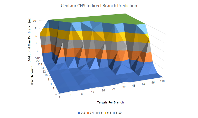

For a core of its size, CNS has impressive indirect branch prediction capabilities. We saw up to 1024 indirect targets handled without much of a penalty, with 256 branches and four targets per branch. Haswell does better when tracking a few branches with a lot of targets, but CNS is better with a lot of branches and a few targets per branch.
Call/Return Prediction
Call and return pairs are a special case of indirect branches, because returns usually go back to where the call came from. To accelerate return prediction, Centaur uses a 7 entry return stack. For comparison, Haswell has a 16 entry return stack, and Zen has 31 entries. CNS’s return stack is small, and it’ll suffer in code with deeply nested calls.
Frontend: Branch Prediction Speed
To speed up branch handling in the frontend, CNS uses a complex, multi-level cache of branch targets. Haswell and CNS can both track 128 branches and handle them with no fetch bubbles. They also look like they hit BTB miss penalties after more than 4096 branches are in play, but the similarities end there.

With under 16 branches, CNS can sustain two taken branches per cycle. It therefore joins Rocket Lake and Golden Cove in an exclusive club of CPUs that can do more than one taken branch per cycle. Intel likely does this by unrolling loops within its micro-op queue, called the LSD (loop stream detector) in Intel’s documentation. Centaur probably has a similar mechanism. Otherwise, they’d need a dual ported instruction cache to achieve such impressive branching performance.
Once we move past 128 branches into the main BTB, Intel and Centaur’s approaches diverge again. CNS seems to use a BTB tied to the L1 instruction cache. Once the loop size exceeds 32 KB, we see a sharp jump in cycles taken per branch. Within the L1i, CNS can do one branch every three cycles. In other words, two fetch cycles are wasted after a taken branch. Perhaps this indicates that CNS’s L1i has 3 cycles of latency. Haswell uses a more modern decoupled BTB, which can track 4096 branches regardless of spacing or L1i hit/miss. Intel’s implementation is also faster, and only wastes one fetch cycle after a taken branch.

For perspective though, CNS does a lot better than AMD’s Zen 2, at least when the two are running at similar clock speeds. Zen 2 can do zero-bubble taken branches with a 16 entry L0 BTB. But after that, it takes steep penalties when it takes branch targets from its larger, slower L1 and L2 BTBs.
Frontend: Instruction Fetch and Decode

MPR’s article says CNS can fetch 32 bytes per cycle from the L1 instruction cache. However, we were only able to achieve this for the 2 KB test size. CNS’s instruction fetch performance ends up looking a bit like Haswell’s, where 32B/cycle fetch can only be achieved for small code sizes, from the uop cache.
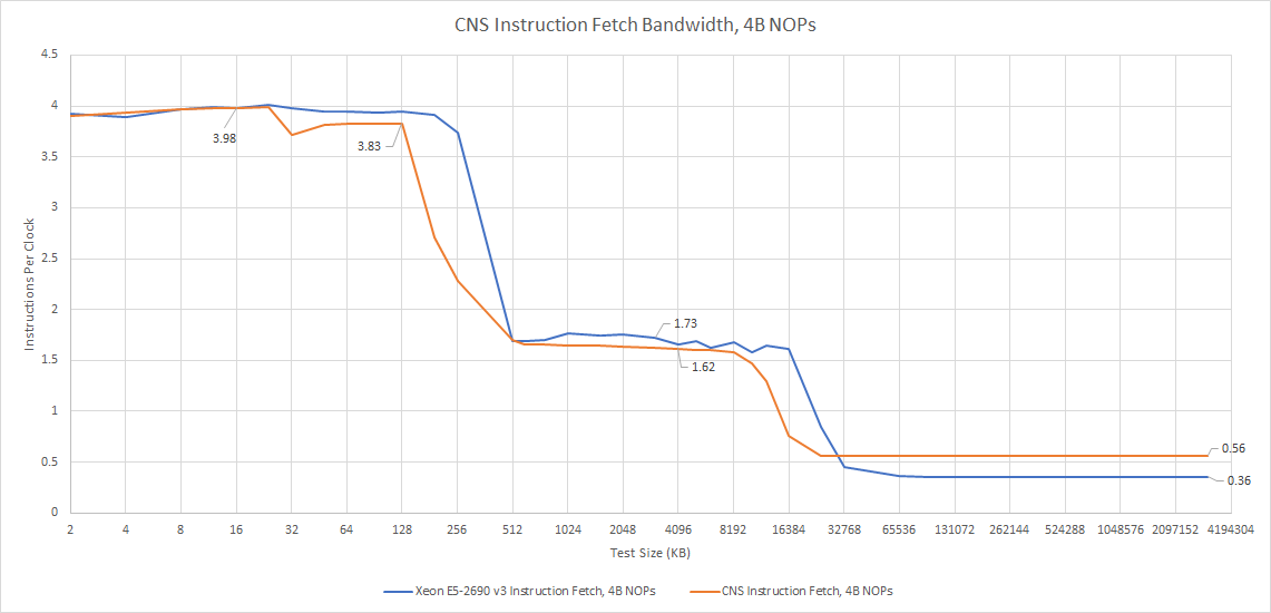
From L2, CNS can sustain around 16 bytes of code per cycle, which is still enough to sustain 4 IPC unless code is dominated by vector instructions. Throughput makes a sharp drop once instructions spill out of L2, but that’s typical behavior for many designs, including Haswell.
CNS can sustain 5 NOPs per cycle, as long as they’re in a tight loop with no more than 24 instructions.

MPR’s article says CNS has a predecode stage that can handle four instructions per cycle. Predecoded instructions are placed into an instruction queue, which feeds the main 4-wide decoder.
One possible explanation for the behavior above is that the instruction queue has 24 entries, and can act as a loop buffer. If code fits within this loop buffer, it bypasses predecode restrictions and can run at 5 IPC, as long as the main decoder can fuse a pair of instructions. This is quite different from Haswell, where the predecode stage is 6-wide, and the loop buffer is behind the main 4-wide decoder.
Like Haswell, CNS can fuse conditional jumps with a previous instruction that sets flags, including arithmetic operations. Unlike other CPUs we’ve looked at, it can also fuse NOPs with adjacent instructions. A fused pair is tracked as a single micro-op in the backend.
Rename/Allocate Stage Optimizations
CNS’s renamer can recognize when an operation will always generate a zero, like when a register is xor-ed with itself or subtracted from itself. For these cases, it can tell the scheduler that it doesn’t need to wait for inputs, allowing more IPC to be extracted. It’s on par with Haswell in that respect.
Unlike Haswell, CNS doesn’t seem to have move elimination capabilities. A chain of dependent register to register move instructions will execute at one per cycle.
Backend: Out of Order Resources
Like any modern high performance CPU, CNS has large buffers to enable out of order execution. Key structures like the register files, ROB, and memory ordering queues are roughly comparable to Haswell’s. Even the scheduler and branch order buffer have similar sizes. Centaur was really targeting Haswell-level performance with this core.

But CNS’s headline feature is AVX-512 support, so let’s look deeper into that. It’s nothing like Skylake-X’s fully featured AVX-512 implementation. Instead, Centaur still uses 256-bit vector registers, and splits 512-bit instructions into two micro-ops. That means CNS doesn’t gain throughput or reordering capacity from using AVX-512.
It could still benefit from AVX-512’s masking features, but that’s problematic as well. On CNS, those mask registers and general purpose integer registers both competitively share the same renamed register file. That’s not great, because CNS doesn’t have a particularly large pool of integer registers to begin with (it’s slightly smaller than Haswell’s). Combined with how 512-bit results consume two vector registers, CNS’s reordering capacity could see much lower limits when AVX-512 is in use.
Backend: Execution Units
Integer Execution
Centaur has not skimped on CNS’s integer units. The core has four ALU pipes like Haswell, but specialized execution units are duplicated across more of CNS’s pipes.

All four of CNS’s ALU pipes can do rotate and shift operations, compared to two on Haswell. Complex bit manipulation operations like PDEP and PEXT can execute at two per cycle on CNS, while Haswell only has one pipe for that. Haswell and CNS can both do integer multiplication with 3 cycle latency, but CNS has two integer multipliers to Haswell’s one. While both CPUs have four ALU pipes on the surface, CNS’s pipes are more flexible, and could enable better throughput especially for applications that take advantage of specialized instructions.
Vector and Floating Point Execution
On the vector execution side, CNS’s setup looks a lot like Haswell’s, except CNS uses separate vector execution pipes instead having the integer execution ports do double duty. Vector integer execution units are spread across three pipes, while FP operations have two pipes to pick from. Again, Centaur doesn’t skimp and execution units are duplicated across more pipes than with Haswell.
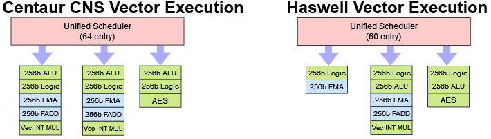
CNS’s floating point unit can execute two 256-bit FP additions or multiplies per cycle, at 3 cycle latency. Haswell’s FP multiplication latency is worse, at 5 cycles. And, Haswell can only do a single FP add operation per cycle at 3 cycle latency. Funnily enough, you could match CNS’s FP addition throughput on Haswell by using FMA ops with a multiplier of 1, albeit at higher latency. Fused multiply add execution is nearly the same across both architectures, with 2×256-bit throughput and 5 cycle latency.
Centaur’s vector integer execution is also more capable. All three pipes can do vector integer addition, while only two of Haswell’s can. Like on the scalar integer side, CNS’s vector side has two integer multipliers, versus one on Haswell. Depending on the exact multiply operation in question, Haswell’s performance can degrade further. For example, pmulld (vector multiplication with 64-bit elements) executes at half rate with a latency of 10 cycles. CNS executes the same operation at ~1.68 per cycle, with 3 cycle latency.
Address Generation
Address generation is one of CNS’s only weaknesses on the execution unit front. CNS has two AGU pipes, each capable of handling either loads or stores. Haswell has three AGUs, allowing it to do two loads and a store in the same cycle.

Centaur still has a few tricks up its sleeve though. It can write 64 bytes per cycle by executing either a single AVX-512 store, or two 256-bit AVX ones. That gives it twice as much store bandwidth as Haswell. In terms of maximum L1D bandwidth, CNS can theoretically hit 128 bytes per cycle with a 1:1 mix of reads and writes. We weren’t able to hit that in our tests, but we did get over 90 bytes per cycle. That’s close to Haswell’s 96 B/cycle theoretical max.
In practice, Haswell’s triple AGU setup probably has a slight edge. Most applications have far more loads than stores, and Haswell’s extra store AGU will reduce pressure on the two general purpose AGUs. This advantage would be minimal though.
Memory Ordering and Store Forwarding
CNS features a rather sophisticated load/store unit. Unlike the VIA Nano and Zhaoxin’s LuJiaZui, it can speculatively execute loads ahead of stores with unknown addresses.
Centaur also has a robust store forwarding mechanism. All cases where a load is completely contained within a prior store are handled with a latency of 7 cycles. It’s also able to complete two loads and two stores per cycle if they’re independent and neither cross a 64 byte cache line boundary. We don’t see that from Intel or AMD until Sunny Cove and Zen 3.
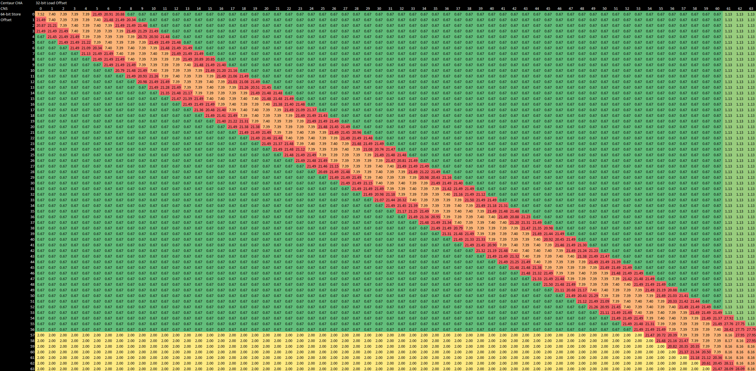
However, latencies are a bit high, especially if forwarding fails. If the load only partially overlaps the store, latency jumps to 21 cycles. Store forwarding latency increases by a cycle if the load crosses a 64 byte cache line. If a load crosses a cache line boundary and store forwarding fails, there’s a 6 cycle penalty.
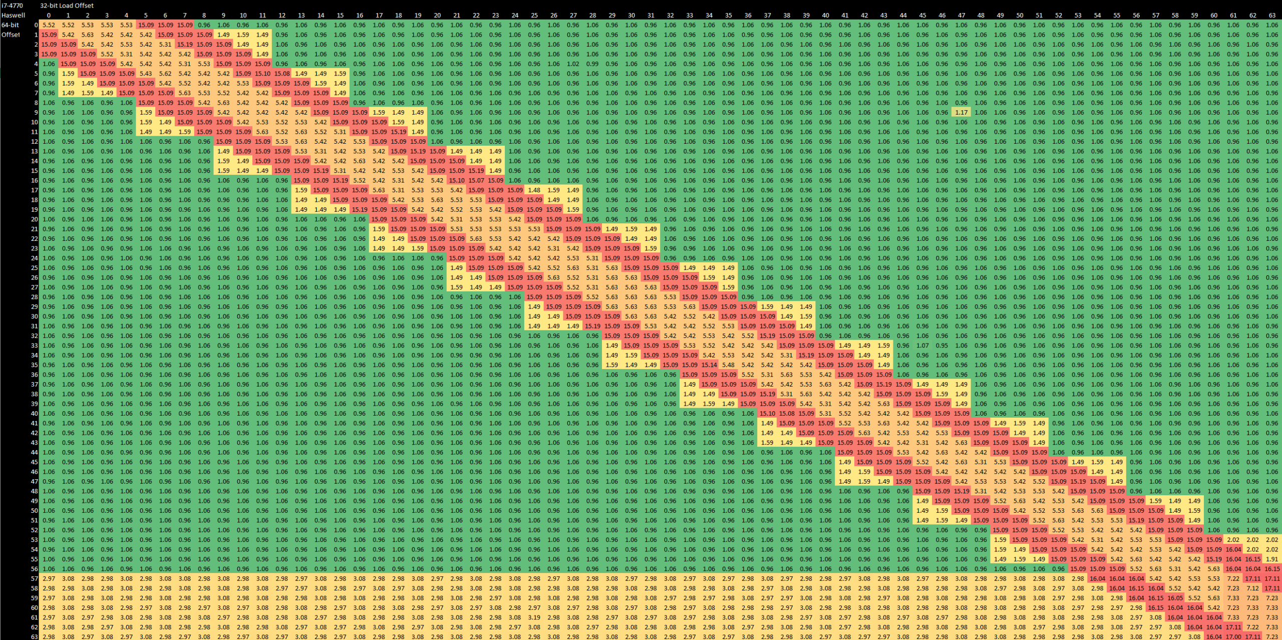
Haswell seems to do a fast check at four byte granularity. If the load and store both access the same 4 byte aligned region, it does a more thorough check that causes a half cycle penalty. That slight penalty applies even if there’s no overlap. Successful store forwarding on Haswell has a latency of 5.5 cycles, while failed store forwarding costs 15. Both latencies are lower than CNS’s, which is quite impressive considering Haswell’s higher clock speeds.
If the load crosses a cache line boundary, Haswell’s store forwarding takes an extra two cycles, and the penalty for a failed store forward increases by one cycle.
Backend: Cache and Memory Access

For the most part, Centaur’s CNS suffers from higher cache latencies than Intel’s Haswell, even when the latter is in a server platform. That’s partially because Haswell is running at 3 GHz, while CNS only runs at 2.2 GHz.

But Centaur falls behind even if we normalize for clock speed. With 5 cycles of latency, Centaur’s L1D is slow. Its L2 is also a cycle slower than Haswell’s. In the L3 region, Centaur again loses both in terms of cycles and absolute time. It only pulls a slight win when we get out to memory.
Things look a bit better for both CPUs if we use 2 MB pages to avoid address translation penalties, but the picture is largely the same. 24 ns of latency is slightly sub-par for a ring servicing just eight cores. Looking at differences in L3 latencies, we can also see that a L2 TLB access takes an extra eight cycles.


In terms of clock cycles, it’s not too much higher than Haswell-E. But the E5-2690 v3 has more cache, more cores, and runs at a higher clock. Intel has done a very impressive job of scaling up the ring interconnect while keeping latency under control.
Bandwidth
CNS’s L1D can do a 64-byte load and a 64-byte store every cycle. We weren’t able to get close to its theoretical bandwidth even with read-modify-write or copy patterns (which give a 1:1 load-to-store ratio), but at least we got more than 64 bytes per cycle.

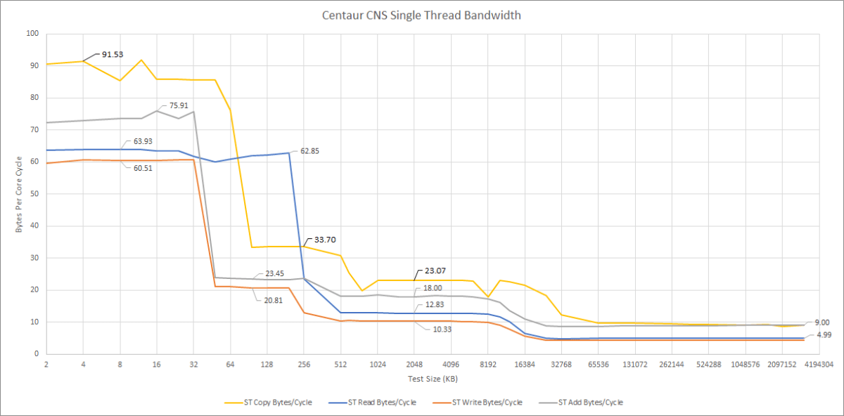
Read bandwidth barely drops when going from L1 to L2, staying at just under 64 bytes per cycle.


Even Intel’s latest cores can’t sustain that amount of L2 read bandwidth. That’s an impressive performance from Centaur’s architecture. Once we get to L3 though, bandwidth takes a sharp drop.

With all eight cores loaded, we see over 1.6 TB/s from CHA’s L1 data caches with a memory copy pattern. L2 bandwidth is highest using a read pattern, at just under 1.1 TB/s. L3 bandwidth hits about 325 GB/s. Finally, we get just above 55 GB/s from memory, with a copy pattern.
On-Die Interconnect and System Architecture

Centaur uses a ring interconnect to connect cores with the L3 cache, and off-die IO. Each ring stop can move 64 bytes per cycle in each direction – twice that of Haswell’s.
Bandwidth Scaling
With eight cores loaded, CNS averages 97.4 bytes per cycle across all eight cores, while Haswell-E gets 81.62 bytes per cycle. CNS’s wider ring does help with bandwidth, but it’s not enough to offset Intel’s clock speed advantage:

As a consolation prize, Centaur’s ring-based L3 is able to provide more bandwidth under heavy load than Ice Lake’s mesh-based cache. Mesh based interconnects tend to have issues clocking up without consuming tremendous amounts of power, resulting in high latency and low bandwidth. Ice Lake’s is no exception.
CHA has a quad channel memory controller that supports DDR4-3200, but memory bandwidth isn’t too impressive. 53 GB/s is well short of the theoretical 102.4 GB/s. Getting close to theoretical bandwidth is hard, because DRAM bandwidth gets lost to refresh cycles and read/write turnarounds. But 52% of theoretical is way too low.

Haswell-E doesn’t do much better. Its first generation DDR4 controller has trouble running at high speeds. Still, Intel’s relatively old architecture shows better memory bandwidth scaling as more cores are loaded. One thought is that CHA wasn’t optimized with CPU memory performance in mind. Centaur has a large NPU taking up a significant chunk of die area, capable of nearly 7 bfloat16 TFLOPs. That could demand a lot of memory bandwidth, especially with the CPU cores active at the same time. Also, the quad channel memory controller could allow more DIMM slots, making it easier to install lots of memory without needing very expensive high capacity modules.
Locks and Cache Coherency
Cache coherency is handled pretty competently with a mechanism that’s likely tied to the L3 slices. The time taken for a core to see a write from another depends on how close both cores are to the L3 slice that the cache line is homed to:

Lock latencies aren’t bad, especially considering CNS’s low clock speeds. Haswell-E ends up being in the same ballpark. On one hand, Intel benefits from higher clocks. But on the other, it’s using a dual ring setup to connect more cores and more cache. More hops across the interconnect generally translates to higher latency.

Clam’s Take
In a vacuum, CNS’s architecture shows how far the Centaur design team has come. CNS is wider and has more reordering capacity than any previous VIA or Centaur architecture. It also implements a grab bag of new microarchitecture features, showcasing the small Centaur team’s design prowess. Loads can be hoisted ahead of stores with an unknown address. Store forwarding is very robust, with behaviour that resembles Sunny Cove’s. There’s a large, unified, multi-ported scheduler. Vector execution units are very powerful for a core of its size. Multiple sets of architectural registers (GPR and AVX-512 mask) are aliased to the same physical register file for better area efficiency. All of this is done in a very compact core:
There’s progress at the system level too. Centaur designed a modern ring interconnect to link the cores with cache and IO. That interconnect enables a large, shared L3, and lets its bandwidth scale to meet the demands of eight cores. Finally, the CHA chip’s quad channel DDR4 controller and 44 PCIe lanes give it more off-chip bandwidth than any previous Centaur design.
But CNS doesn’t exist in a vacuum. Haswell level IPC is great. What’s not great (for Centaur) is that Haswell clocks much higher. Intel also refined their ring bus over several generations, letting it support higher core counts and scale to higher bandwidth, even with narrower links between ring stops. Centaur’s architecture, while ambitious, would have a tough time against Haswell.
Worse, Centaur’s CHA chip still wasn’t on the market in 2021. That put it up against Intel’s Icelake-SP based Xeons, and AMD’s Zen 3 based EPYC chips. Centaur is a small company with limited resources, and is a process node behind. In a pure CPU versus CPU battle, they stood no chance.
But Centaur knew that. That’s where NCore comes in. It’s a beefy machine learning accelerator capable of 6.8 trillion bfloat16 operations per second. Centaur wanted to pair their CNS architecture with NCore to create a uniquely competitive product. Core for core, CNS can’t take on Skylake or Zen 2, but it’s more than adequate for driving an ML accelerator. For context, Intel targeted 5G base stations (which counts as “edge”) with Snow Ridge. Snow Ridge has Tremont cores running at 2.2 GHz. ARM targets edge applications with Neoverse E1. CNS would stand up well against them, especially with vectorized workloads.
Placing the NCore on-die also reduces latency, and leaves PCIe lanes free for other IO. On the edge, that’d undoubtedly be a ton of networking bandwidth. CNS and NCore together make sense if you want a server with powerful inference capabilities, but had more moderate demands for CPU performance and didn’t have the space or power budget for external ML accelerators.
I suppose that market never materialized. Or if it did, it wasn’t enough to save Centaur. Then, Intel snapped up Centaur’s design team, because those engineers are very good at doing a lot with limited resources. CNS is a testament to that.
Final Words
In conclusion, while it is sad to see a CPU design house close shop, Centaur would not have competed with either AMD or Intel. Even if Centaur had launched a system with the CNS core in 2017, both Intel and AMD had more expandable systems in the form of Skylake-X and Zen 1 EPYC because CNS can only scale to 2 sockets with a total of 16 cores versus Skylake-X’s max of 224 cores across 8 sockets and EPYC’s max of 64 cores across 2 sockets.
However in Centaur’s planned release year of 2020, like Clam said, things were not looking good for either Centaur or the CNS core. And in late 2021, the scene was looking ever grimmer for Centaur and they decided to close up shop with a buyout by Intel for 125 million US dollars.
Now, the buyout does not necessarily mean that the CNS core is dead. The wildcard in all of this is Zhaoxin. Zhaoxin has been very quiet during this acquisition of Centaur by Intel but they have proven that they can improve on Centaur’s already existing designs with Lujiazui.
In 2018, Zhaoxin claimed to be able to catch up to AMD’s then fairly new Zen 1 architecture with their KX-7000 series of CPUs and I suspect that they were planning on using the CNS core to do that. This hypothesis does have creditable evidence in support of it due to the prototype boards using the ZX-200 as their southbridge and that VIA transferred IP to Zhaoxin in October of 2020 which included CPU IP. Now, whether or not Zhaoxin can clock the CNS core to the 3.5+ GHz that a modern desktop CPU needs in order to be competitive is a different story.
Regardless of if Zhaoxin could get CNS up to 3.5GHz, the point is moot. This is not early 2019, it’s early 2022 so this hypothetical 3.5GHz CNS would not be able to get near to either AMD’s or Intel’s current architectures let alone what will be out in roughly 6 to 9 months.
But back to the buyout of Centaur by Intel, the 125 million dollar question is why? Why did Intel buy the Centaur design house? To be frank, we have no idea. Centaur was no threat to Intel or even AMD. There are a few possible reasons that I can think of:
Intel wanted some IP owned by Centaur such as NCore
Intel wanted the Centaur engineers because as Clam said, they seemingly can do a lot with very little resources
Intel wanted a good enough x86 CPU core on a TSMC node for projects where the fastest CPU core is not required and Intel wants to use x86 compatible cores
And the most cynical reason is that Intel just wanted one fewer company with the x86 license, although VIA still has the Cyrix license as far as I know
Unfortunately, the actual reason as to why Intel acquired Centaur may never be known due to Intel being very tight lipped as to why they gobbled up Centaur. This is quite possibly the end of an era that most didn’t know still existed. Maybe Zhaoxin will take up the mantle of the third high performance x86 design house that has been held by Cyrix and Centaur or maybe we will be reduced to two high performance x86 design houses in AMD and Intel. I cannot predict the future but what I do know is that this article is at its end.
If you like our articles and journalism and you want to support us in our endeavors then consider heading over to our Patreon or our PayPal if you want to toss a few bucks our way or if you would like to talk with the Chips and Cheese staff and the people behind the scenes then consider joining our Discord.