Popping the Hood on Golden Cove
Alder Lake (ADL) is the most exciting Intel launch in more than half a decade. For the first time since Skylake, Intel has launched a competitive desktop microarchitecture. But I’m sure you all know that already from other sites that are able to do launch day reviews.
Here, we’re going to deep dive ADL’s P-core architecture, Golden Cove. Primarly, we’re going to compare Golden Cove to its direct predecessor, Sunny Cove, and use that as a basis for analyzing Intel’s design choices. In a few cases, we’ll show data from Skylake and AMD’s architectures to put Intel’s progress in perspective. Finally, we’re going to skip introducing Alder Lake and Golden Cove, as other tech sites like Anandtech and Tom’s Hardware have already done that. But in short, Golden Cove cores target peak performance.
Block Diagram
To start, let’s look at Golden Cove from a mile up. Some of the our data comes from Intel’s Architecture Day presentation. The rest comes from our own testing on an i9-12900K. We don’t have a board that allows AVX-512 instructions, and those instructions fault on Golden Cove, so unfortunately that won’t be covered. And of course, treat this diagram as a rough approximation, because testing is hard.

And let’s do the same with Sunny Cove, tested on a Xeon 8370C in an Azure VM:
At a high level, Golden Cove is both wider and deeper. Instruction reordering capacity (the reorder buffer) has gone up by a staggering 45%. Various queues and register files get bigger too.
Now, let’s take a trip through the Golden Cove pipeline. We’ll start from the very beginning, at the branch predictor.
The Branch Predictor: Steering the CPU’s Pipeline
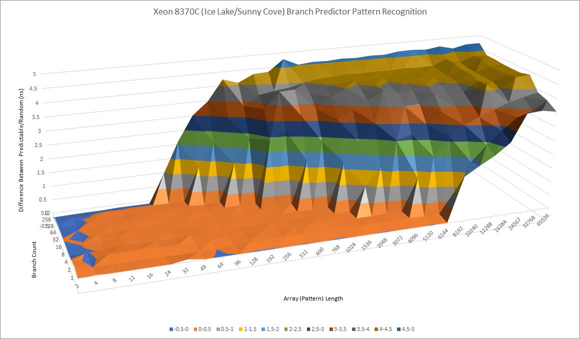
Intel’s Architecture Day presentation claimed “improved branch prediction accuracy” for Golden Cove. Let’s have a look at how well Intel’s newest architecture can recognize branch direction patterns. And for perspective, compare that with Sunny Cove.
While the difference isn’t huge, Intel has clearly tweaked Golden Cove’s prediction algorithms. After the repeating random pattern goes over 6144, Golden Cove’s time per branch doesn’t jump as sharply. Here’s Skylake for comparison:
Skylake is blown out of the water. Golden Cove can recognize much longer patterns, and copes better when a lot of branches are in play. Now, let’s examine AMD’s direction predictors:
Zen 3 can recognize longer patterns than Golden Cove. Compared to Zen 2, Golden Cove is roughly equal when one branch is involved (factoring out Zen 2’s huge L2 TAGE predictor override penalty). Both AMD architectures can better cope with tons of branches. With 512 branches in the loop, Zen 2 and Zen 3 can hold up well when the repeating pattern is 64 or 96 long, respectively. Golden Cove suffers once the pattern length exceeds 48.
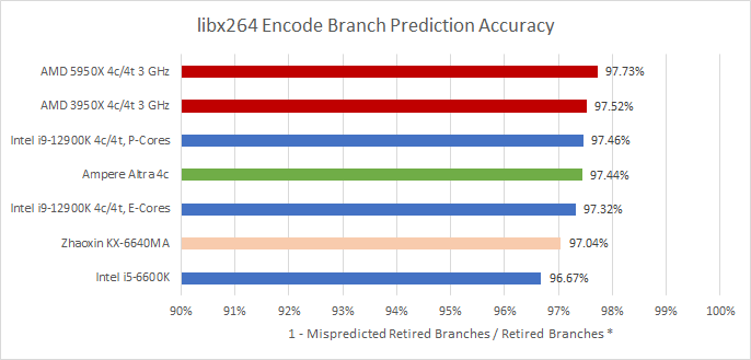
But enough with picking apart the predictor with microbenchmarks. Let’s see the impact of Intel’s changes in practice:
Golden Cove’s predictor performs very well and is a clear step above Skylake’s. However, it’s still a hair behind AMD’s branch predictor in our testing.
BTB Speed and Capacity – How Fast does the Rudder Move?
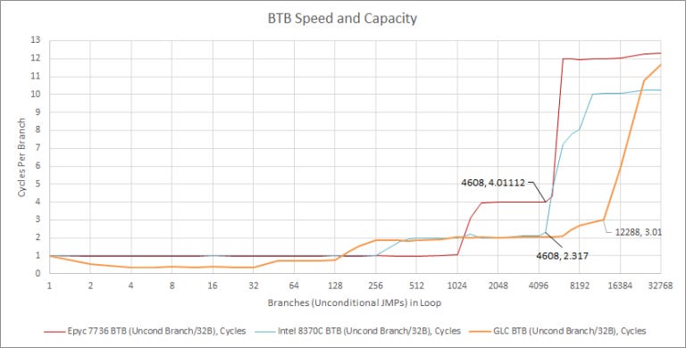
Of course branch predictor accuracy is important, but a good predictor should deliver branch targets quickly as well. To do this, the predictor keeps a cache of branch targets, usually referred to as the branch target buffer (BTB). Intel has equipped Golden Cove with a ludicrously large BTB.
Golden Cove’s BTB seems to have three levels. Missing in one level and hitting in the next incurs a 1 cycle penalty, which is quite fast compared to AMD’s 3 cycle penalty for a L2 BTB hit. And like Sunny Cove (in Rocket Lake form, not Ice Lake for unknown reasons), Golden Cove can unroll loops within its uop queue, giving it an incredible throughput of two taken branches per cycle. In a sense, Intel’s uop queue acts like a tiny trace cache, reducing branch overhead for small loops without needing loop unrolling from the developer or compiler.
However, Zen 3 can still have a speed advantage in some cases. It can track up to 1024 branches and handle them back to back, with no lost cycles between them. Golden Cove can handle 128 branches with roughly 1-per-cycle throughput. That’s equivalent to Haswell’s ability, but is a regression compared to Sunny Cove. Intel probably made tradeoffs to get such a large BTB working above 5 GHz.
Return Prediction
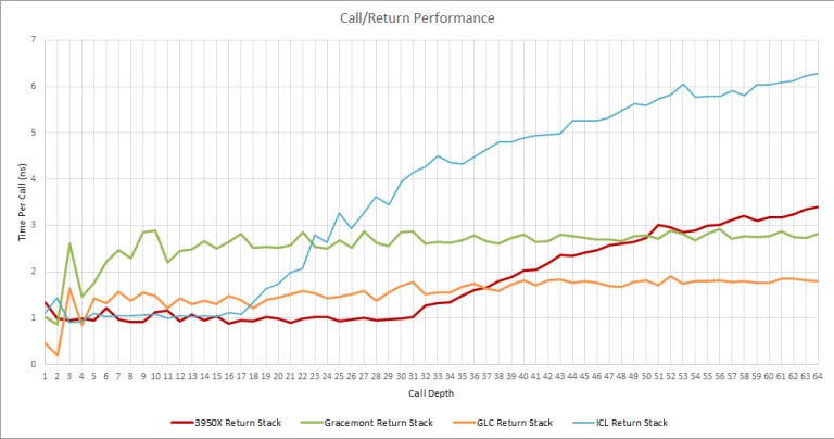
Golden Cove’s return prediction behavior is strange. There’s no clear jump up, even when we increased the number of call/return pairs to 128. But when calls go more than two deep, Golden Cove is rather slow at handling returns. Sunny Cove and Zen 2/3 in comparison are faster at returns, even at a lower clock – at least until their return stack overflows.
Instruction Fetch
Once the branch predictor has told the CPU where the next instruction should be, it’s time to fetch it. To accelerate this, Golden Cove gets a bigger 4K entry uop cache, up from 2.25K in Sunny Cove and 1.5K in Skylake. Uop cache bandwidth has improved too. Golden Cove can fetch 8 micro-ops per cycle from that cache, matching Zen in that respect. For comparison, Sunny Cove and Skylake could only fetch 6 micro-ops per cycle from their uop caches.
If there’s a micro-op cache miss, Golden Cove has six instruction decoders. To feed those decoders, Intel has increased L1 instruction cache bandwidth to 32 bytes/cycle. That’s a notable improvement compared to Sunny Cove and Skylake, which could only fetch 16 bytes/cycle from their L1i caches and used 4-wide decoders.
We wrote a test that measures instruction fetch bandwidth with 8 byte NOPs, specifically 0F 1F 84 00 00 00 00 00. The test fills an array with those, puts a return (C3) at the end, and times how long it takes to execute in a loop. Golden Cove’s pipeline is 6-wide, so we should get 48 bytes/cycle if instruction bandwidth isn’t a bottleneck. And it shouldn’t be as long as we hit the uop cache, which can deliver 64 bytes of instructions per cycle.

Strangely, we’re not able to see Golden Cove’s larger uop cache with our test. In fact, the shape of Golden Cove’s curve is similar to Skylake’s, suggesting a large number of uop cache misses with just over 1024 NOPs (8 KB) in the loop. However, this is largely mitigated by Golden Cove’s higher bandwidth L1 instruction cache.
Past L1, all CPUs here can read 16 bytes/cycle from L2. The average x86 instruction is 3-4 bytes long in integer code (our test with 8 byte NOPs is more applicable to very AVX-heavy code). 16 bytes/cycle is therefore enough instruction bandwidth to feed the core with 4 to 5 instructions per cycle. In L3, results are similar too if we ignore Ice Lake, where bandwidth is probably limited by the mesh interconnect.
Feeding the Execution Engine – Rename/Allocate
Once instructions have been brought into the core and translated into the CPU’s internal format, we have to allocate resources in the backend to track them and enable out of order execution. This stage is called the renamer because it renames ISA registers to physical ones in the CPU’s backend, removing false dependencies. In modern architectures, the renamer can pull off some tricks to expose even more parallelism to the backend.
Intel first introduced move elimination in Ivy Bridge, but that mechanism got a lot more robust in Sunny Cove. Sunny Cove’s ability to eliminate chained MOVs is only restricted by the renamer’s width. Golden Cove carries that forward, but increases rename width to 6 instructions per cycle. Golden Cove’s move elimination is thus a match for Zen 3’s, and represents a lot of forward progress compared to Skylake.
But move elimination is hardly the only trick in the book. Programs quite often set registers to zero, in order to clear them. Golden Cove can recognize all of the zeroing idioms we tested. And it doesn’t just recognize these as special cases of independence – it eliminates them so they don’t need an ALU port to execute.
In contrast, Zen 3 can recognize zeroing idioms as independent and removes false dependencies between them. But only the XOR case (exclusive OR of a value with itself is always zero) and subtraction cases are eliminated. The “move immediate value of zero to a register” case still occupies ALU pipes, and throughput is bound by Zen 3’s four ALUs.
Extracting Parallelism – GLC’s Out of Order Engine
The point of large out-of-order buffers is simple – they let the CPU track instructions ahead of a stalled one, and hopefully keep the execution units busy instead of simply getting stuck on one long latency instruction. But allocating these resources is much more complicated, and some structures are more expensive than others. Travis Downs has an excellent explanation of when each structure can limit the out-of-order window, so we’ll jump right to what Intel has done with Golden Cove.
Golden Cove’s reorder buffer is a staggering 45% larger than Sunny Cove’s. This structure tracks all micro-ops in the backend until they’re retired (exceptions checked for and results made final). To take advantage of the bigger reordering window, other structures have received size increases too. Intel treated the FP register file, load/store queues, and superqueue very nicely. The fill buffer and branch order buffer got more modest increases, but should still be adequate. GLC’s scheduler gets a comparatively smaller boost, but that’s understandable because the scheduler seems to be a very expensive structure. However, Intel didn’t give the integer register file any love.
From our testing, it actually seems a bit smaller on Golden Cove. Intel probably didn’t shrink this important structure, so I’m giving them the benefit of the doubt. In any case, Intel’s decision to not equip Golden Cove with more integer registers is baffling.
The table below shows reordering capacity for as a percentage of maximum reordering capacity (ROB size), for major instruction categories. For reference, we put two workloads through Intel SDE to get executed instruction counts, and categorized those instructions.
Golden Cove’s integer register file stands out, and not in a good way. In pure integer loads, GLC may struggle to make good use of its headline grabbing 512 entry ROB because it’ll run out of integer registers before the ROB fills. However, it should not be a major issue with floating point and vector workloads, where a much smaller fraction of instructions generate integer results. And, Golden Cove’s measured reordering capacity there still exceeds Zen 3’s by over 40%.
Execution Units
Execution units are rarely a bottleneck on modern CPUs. Usually, branch prediction along with cache and memory latency are limiting factors. That doesn’t look like an exception on Golden Cove, since its execution units look ample and well distributed across ports. So here, we’re going to look both at scheduling queue layout, which can have a significant effect on performance. And we’ll check out the register file inputs required to feed execution ports for a view into Intel’s (and AMD’s) strategy.
Golden Cove features five integer execution units – the most in any x86 CPU to date. I wonder if that explains why the integer register file didn’t get bigger. Feeding five ALUs with two inputs each would require ten integer register file ports. Golden Cove’s address generation units would require another five integer inputs. Perhaps implementing so many ports made a integer RF size increase too difficult and expensive. Some of the register file ports might be shared between several execution ports. But we were able to use all five integer ALUs at once, so the integer register file has at least ten read ports.
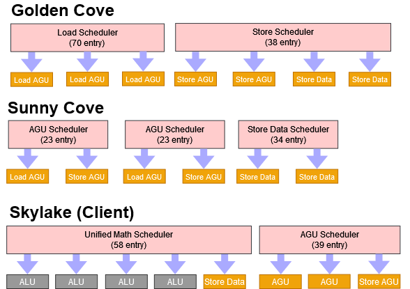
Like previous Intel designs, Golden Cove uses a unified scheduler for math operations, and puts address generation units (AGUs) on a separate scheduling queue. In contrast, AMD uses a distributed scheduler for integer math, but shares them with AGU pipes. Speaking of AGUs…
AGU count also gets a boost on Golden Cove. Intel’s P-Core can generate addresses for three loads and two stores per cycle, again setting a record for x86 CPUs.
Unlike the math side, the AGU scheduler layout has changed pretty dramatically over the past two generations. Intel still seems quite busy with optimizing it. The same applies to AMD:
For address generation, Golden Cove can handle three loads and two stores per cycle. The load and store AGUs are separate on Intel’s diagram, unlike AMD where three AGUs handle both loads and stores. Now, let’s look at the floating point and vector side.
Golden Cove puts its floating point units behind three ports, an improvement over previous Intel architectures that only had two ports for floating point loads. But more impressively, Golden Cove can do floating point additions with two cycle latency. We’ve seen that before in low frequency designs like VIA’s Nano. But Golden Cove is doing this at over 5 GHz. That’s incredible, and Intel’s engineers should be proud. AMD’s Zen 3 clocks lower, but still takes three cycles to generate a floating point addition result. The situation flips with floating point multiplies, where Golden Cove has 4 cycle latency compared to 3 cycles on Zen 3.
AMD and Intel can both do vector integer addition with 1 cycle latency. However, Golden Cove’s vector integer multiplier has 10 cycle latency (with packed 32-bit integers), just like older Intel CPUs. That’s far worse than Zen 3’s 3 cycle latency, or Zen 2’s 4 cycle latency.
Like previous designs, Intel uses a unified scheduler for both integer and vector/FP operations. A unified scheduler is always more efficient for a given number of entries, and is easier to tune as well. AMD uses split scheduling queues, which might be easier to implement in silicon, but requires careful tuning to make instructions for most loads are well distributed among the queues.
AMD’s Zen 3 features four ports for vector/FP loads. While throughput for individual floating point math operations (add, multiply, fused multiply-add) are the same as Intel’s, Zen 3 features an additional vector integer unit. In very high IPC vector/FP code, Golden Cove could be limited by execution ports more than Zen 3 is. Thankfully for Intel, execution port throughput is rarely a bottleneck, and Intel’s past chips have been fine with an even weaker port layout. AMD’s port advantage becomes less significant with fused multiply add (FMA) operations, which require three inputs from the register file. AMD doesn’t have enough vector register file bandwidth to feed both FMA units and keep the other two ports busy. Let’s dig deeper into that.
Golden Cove’s vector register file probably has eight read ports1 and three write ports. Zen 1 and 2 have at least eight read read ports and four write ports. Zen 3 likely has even more, to feed its two extra FPU pipes. Intel probably found it relatively easy to increase their vector register file size, since there are fewer ports. AMD on the other hand has remained at 160 vector registers for Bulldozer, Piledriver, Zen 1, Zen 2, and Zen 3. Steamroller and Excavator have 176 vector registers, but only have three FP pipes that need a maximum of eight read ports and three write ports. Though to be fair to AMD, their vector register renaming capacity still covers enough of ROB capacity, so changes there aren’t required – yet. In any case, it’s really interesting how AMD and Intel have taken opposite approaches to register file design.
Memory Subsystem: Massive Bandwidth, High Latency
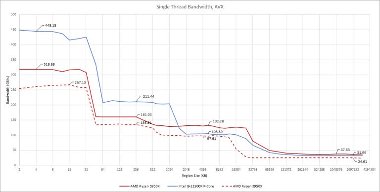
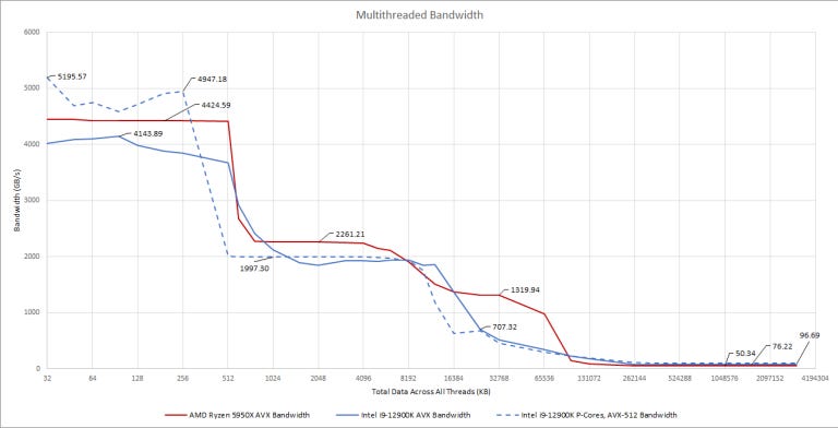
Right off the bat, Alder Lake performs very well for a 8+8 design. Its L1D and L2 bandwidth are a close match for AMD’s 3950X, and not too far off from the 5950X. AMD’s L3 design still gives a lot more bandwidth than Intel. But the difference isn’t as huge as it might seem. AMD’s design uses 16 L3 slices, split as 8+8 (5950X) or 4+4+4+4 (3950X), while Intel uses 12 slices in a unified cache. Both Intel and AMD scale L3 bandwidth by trying to evenly distribute accesses across slices, with each slice able to deliver 32 bytes per cycle. In terms of per-slice bandwidth, AMD only has a 39.9% lead.
At larger sizes, DDR5 helps Alder Lake pull ahead. With DDR5-6200 (below), we saw Alder Lake achieve 96.6 GB/s with a 3 GB test size. That’s almost double the memory bandwidth we saw Zen 3 get with DDR4.
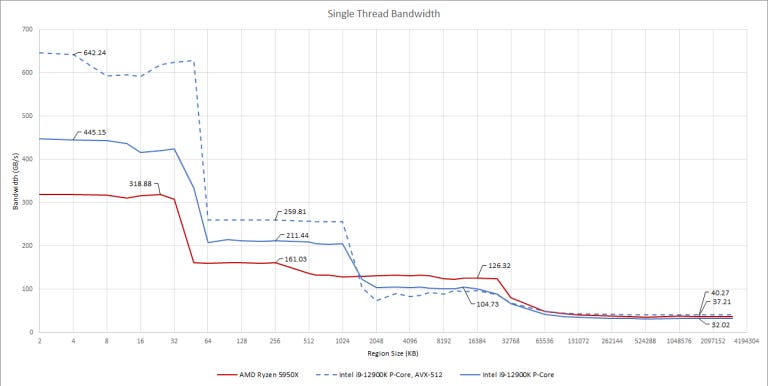
Looking at a single thread bandwidth on Golden Cove, we see three 256-bit vector loads per cycle from L1D. That’s impressive, and explains how Intel can compete against AMD chips sporting more “P-Cores”. For comparison, AMD’s Zen 3 can do three loads per cycle, but only two of those can be vector loads. Golden Cove also has a wider 64 byte per cycle path to L2, while AMD uses a narrower 32 byte per cycle path. If you have a vectorized program that fits in core-private caches, Golden Cove gives you massive bandwidth.
AVX-512 Bandwidth
AVX-512 is not officially supported, but can be used with some boards if E-cores are disabled.
Golden Cove can do two 512-bit loads per cycle. It’s like Skylake-X but at 5.2 GHz, which means absolutely insane L1D bandwidth. With our test in MT mode, eight Golden Cove cores actually get more L1D bandwidth than 16 Zen 3 ones. In the L2 region, Intel gets slightly better bandwidth efficiency with AVX-512 at just above 78% of the theoretical 64 bytes per cycle, compared to 63.5% with AVX. Past L2, AVX-512 doesn’t provide a bandwidth advantage.
At every memory hierarchy level, Golden Cove is a bandwidth monster. It has large, high clocking L1 and L2 caches with very wide busses. AMD only maintains a bandwidth advantage in L3. For workloads that aren’t cache friendly, Intel’s DDR5 memory controller is something AMD can’t match right now.
Latency

High bandwidth at high clocks doesn’t come for free. At all cache levels, Golden Cove has to cope with more latency than Zen 3. In exchange, Golden Cove’s L1 and L2 caches are larger than AMD’s, and deliver more bandwidth.
If we assume Golden Cove ran at 5.2 GHz, and Zen 3 ran at 5.05 GHz, we can also see latency in terms of cycles.

This cache latency explains why Golden Cove needs larger out of order resources. Remember the “long latency instructions” mentioned earlier? The most common ones are simply memory accesses that miss cache. Let’s look at ROB size and memory access latency together, with a little application of Little’s Law. This law states that queue length is equal to arrival rate multiplied by latency. We’re going to apply this to instruction throughput, and use ROB size as queue length (assuming other queues are properly sized to prevent them from filling before the ROB).
Golden Cove’s huge ROB is more than adequate to absorb its extra cache latency, without falling behind Zen 3. Meanwhile, Zen 3’s ROB looks tiny both relative to its cache latency and Golden Cove’s ROB. This is a simplistic look of course. We’re planning to evaluate Intel’s cache design later on with simulations.
First Thoughts
Intel made Golden Cove an absolutely giant design. As shown by other reviews, Golden Cove’s single threaded performance beats Zen 3’s, while the i9-12900K is very competitive with AMD’s high core count desktop parts. After years of Skylake refreshes (and Rocket Lake), Golden Cove is refreshing to see.
Golden Cove looks particularly well tuned for floating point and vector workloads. The FP port layout got tweaked, FP addition latency is an impessively low 2 cycles, and the vector register file is gigantic. Vector loads get massive bandwidth from Golden Cove’s core-private caches, and carving work into L2 sized chunks (cache blocking) is easier with the large 1.25 MB L2. Even the extra ALU pipe looks aimed at FP/vector loads. Three of Golden Cove’s five ALU ports serve FP/vector execution units. Vectorized workloads still execute a lot of scalar integer instructions to handle loop counting, branching, and address calculation. Two dedicated ALU ports instead of one can help crunch through these integer instructions.
For integer loads, Golden Cove’s extra ALU and tweaked renamer should still boost performance. But I feel Intel left some integer performance on table to stretch Golden Cove’s design across Alder Lake and Sapphire Rapids. Golden Cove’s higher latency caches mean it needs more reordering capacity to prevent latency from becoming a bottleneck. Intel could have done better in integer workloads by ensuring the execution pipes are better fed, rather than spamming more ALUs. I wonder if Intel made these compromises because Golden Cove had to serve double duty in Sapphire Rapids.
To conclude, let’s look at Golden Cove and Zen 3 to see each company’s strengths and weaknesses. Intel’s strong points are:
Wide core with very deep reordering capacity
Massive cache bandwidth and better memory bandwidth too if DDR5 is used
Large L2
Huge BTB with relatively low latency for its size, likely able to cover instruction prefetches well into L2
AVX-512, if you can use it
Tweaked renamer that matches or beats AMD’s in all respects
But Intel’s weaknesses are:
Higher latency at all cache levels, compared to Zen 3
Disproportionately small integer register file, compared to the size of the ROB
Branch predictor is slightly worse than AMD’s
And now for Zen 3’s strengths:
Larger zero-bubble BTB capacity
The best branch predictor we’ve seen so far
High bandwidth and low latency L3
As for Zen 3’s weaknesses:
Smaller core-private caches, relative to Willow Cove and Golden Cove
Smaller out-of-order resources are less able to handle L3 and memory latency
Looking Forward
Golden Cove builds on Sunny Cove’s strengths while knocking out some of AMD’s remaining advantages. With Alder Lake’s launch, Intel has regained the single thread performance crown. But it’s not a knockout punch. Zen 3’s branch predictor is still better, and enjoys better cache latency. Both of those factors let Zen 3 make better use of its smaller resources. Or alternatively, those remaining Intel weaknesses blunt the impact of Golden Cove’s huge out-of-order queues. Intel still comes out on top in the end, but Zen 3 is not as far behind as a simple block diagram would suggest.
Alder Lake comes about a year after Zen 3, meaning the ball is firmly in AMD’s court. Zen 4 is rumored to launch next year with AVX-512 support. We’re excited to see whether AMD can regain the single thread performance crown with their next release.
If you like our articles and journalism and you want to support us in our endeavors then consider heading over to our Patreon or our PayPal if you want to toss a few bucks our way.
Appendix
1. Vector Register File Bandwidth
There’s no documentation on Intel’s vector register file bandwidth. But based on experimentation, Haswell almost certainly doesn’t have eight read ports. We got 2.41 IPC with a sequence of FMA and vector integer add instructions in a 2:1 ratio. That corresponds to 6.43 vector register reads on average. But if every other FMA instruction takes one input from the L1 data cache instead of a vector register, we see 2.93 IPC, indicating we’re just about saturating all three vector pipes. In terms of 256-bit inputs, that’s 7.81 per cycle. Thus, Haswell’s vector register file probably has seven read ports.
On Sunny Cove, we were able to get 3 IPC even without making half of the FMA instructions load-ops. We assume this carries forward with Golden Cove, giving it eight read ports from the vector register file.
Revisions
12-2-2021 – Updated the vector register file section – Zen has eight read ports from the vector register file. Originally I misread AMD’s optimization guide.


