
Details on the Gigabyte Leak

Recently, a ransomware group leaked data from Gigabyte in an attempt to extort payment. That’s been well covered by other outlets (please everyone, secure your networks), so here we’re focusing on Zen 4 technical details from the leak.
Sadly there’s not a lot on fundamental core changes however, there is some stuff we can get from the data provided in the leak. Performance counter event unit mask descriptions show Zen 4 still has four integer scheduling queues like Zen 3 along with the BTB is still being split into two levels. As covered by other outlets, Genoa supports AVX-512F, VL, BW, CD, IFMA, DQ, VPOPCNTDQ, BITALG, VNNI, VBMI, VBMI2, and BF16 (bfloat16) which puts it at roughly an AVX512 featureset level of Ice Lake Server in terms of AVX512 exclusive instructions.
Cache and TLB Parameters

Zen 4’s doubled L2 size is welcome news, and should increase hitrate. Unlike Willow Cove’s 1280 KB 20-way L2, AMD opted to retain an 8-way associative L2 and simply double the number of sets. Generally, caches with lower associativity have an increased chance of conflict misses and thus lower hitrates but in return, they can do lookups faster and/or with lower power because fewer tags have to be checked per access. Compared to Willow Cove, Zen 4 will likely have a lower latency L2 at the expense of slightly worse hitrate.
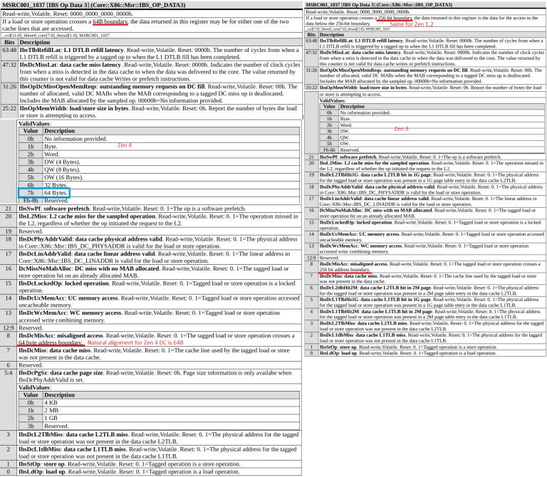
The 3072 entry L2 DTLB lets Zen 4 cache 4K page translations for 12 MB of memory, up from 8 MB in Zen 2/3. Zen 4 also has page coalescing capability. There weren’t specifics on whether this mechanism changed in Zen 4, though performance counter unit mask descriptions indicate it’s still present. Assuming Zen 4 can coalesce up to four consecutive 4K pages like Zen 2 and 3, the 3072 entry L2 DTLB can cover up to 48 MB which is great news. While Zen 2/3’s 2048 entry L2 DTLB already preformed reasonably well, more is always better.
The Zen 4 PPR also says the L2 tag and state arrays use 7 ECC bits per 42 tag bits, which could be useful for calculating SRAM density.
AVX-512 Throughput Speculation
While the L1D size and associativity has not changed, its natural alignment has changed to 64 bytes instead of 32 bytes on previous Zen generations. This doesn’t guarantee 64 byte (512-bit) per cycle ports to the data cache – Zen 1’s data cache had a natural alignment of 32 bytes but 16 byte per cycle (128-bit) load and store ports. Regardless, Zen 4 should achieve higher load/store throughput than previous generations because memory operations that cross a 32 byte boundary without crossing a 64 byte one won’t incur an extra data cache access.
From Zen 4’s instruction based sampling data fields, a single micro-op can access up to 64 bytes which breaks a long running trend where the first generation of AMD CPUs to support a wider width FPU decoded them into two micro-ops – at least for memory operations and because most AVX(512) math instructions can have a memory operand, there’s a good chance 512-bit math operations aren’t split into two 256-bit ops as well.
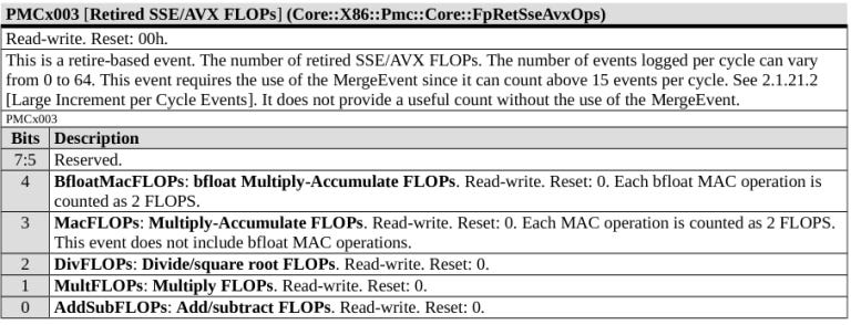
Zen 4’s retired FLOPs performance event can only increment by up to 64 FLOPs per cycle thus we don’t expect more than 2×512-bit FP32 FMA throughput, or 64 FP32 FLOPs per cycle. However this means that bfloat16 throughput is likely only 1×512-bit, or 64 bfloat16 FLOPs per cycle.
Personally, I think Zen 4 might have a single 512-bit FMA unit that can be addressed as 1×512 or 2×256, in a setup similar to Sunny Cove’s. While massive vector throughput is nice to have for certain workloads, it comes with high power and area costs. Simply having 512-bit micro-ops already provides a large advantage in conserving out-of-order resources and more efficiently using the memory subsystem. Pipe configuration might be similar to prior Zen generations with 2 FMA pipes and 2 FADD pipes, but with 512-bit capability on at least one FMA pipe.
Memory Subsystem: Thinking Big
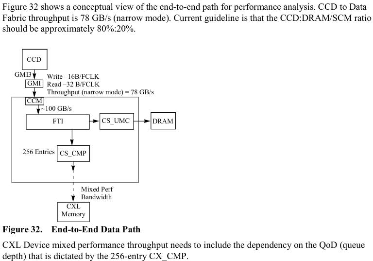
Storage class memory (SCM) gets first class treatment on Genoa. Performance monitoring events for L1 cache refills can track SCM as a source, alongside L2, L3, and DRAM. Instruction Based Sampling can also identify whether a micro-op loaded data from ‘DRAM address map with “long latency” bit set’. While faster than traditional SSDs, SCM, which most people have heard of in the form of Intel’s Optane DIMMs, is expected to have much higher latency than DRAM, which makes SCM a possible candidate for “long latency” DRAM.
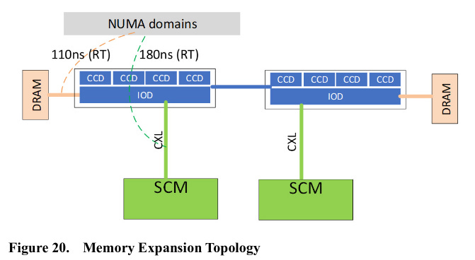
“Extension Memory” shows up as another new data source category, with GenZ (links to possibly external memory) among the examples. Finally, “Peer Agent Memory” is mentioned. It’s not clear what a peer is, but it could refer to accelerator devices.

From a mile up, Zen 4’s performance monitoring capabilities have been enhanced to deal with technologies that enable very large memory configurations. SCM aims to fill the gap between slow SSDs and fast DRAM by offering data persistence with speeds and capacities between that of DRAM and traditional flash based storage. “Extension” and “Peer Agent” memory probably allow scaling memory capacity outside a physical single server blade. The best part is all of those memory sources can be transparently addressed by user programs.
While it’d be extremely cool if parts of new Genoa based supercomputers can be used as giant shared memory systems, AMD says memory pooling is outside Zen 4’s scope.
Handing More Bandwidth
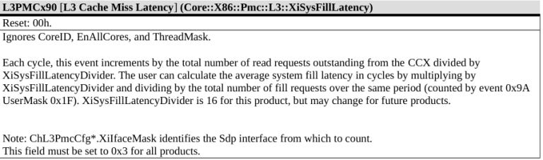
Each CCX/CCD might feature two Scalable Data Ports (SDP), or links to Infinity Fabric (IF). Setting the SDP interface mask to 0x3, or 11 in binary, would mean selecting two interfaces (with each bit controlling whether its respective interface is selected for monitoring). Like Zen 2 and Zen 3, the CCX/CCD links remain 32 bytes wide for loads and 16 bytes wide for stores.

Zen 4 in Genoa (server) form supports up to 12 channels of DDR5-5200. To increase bandwidth available to a single CCD, it seems AMD has opted to add more IF links to each CCD. ‘Narrow mode’ may be a way to save even more power by disabling one of the IF links when high bandwidth isn’t required.
AMD has also enhanced the rest of the IO subsystem.
LCLK is the clock domain for the IO hub. Compared to Milan and Rome, Genoa sees a 53% LCLK frequency increase, and two IO hubs instead of one. That should greatly increase IO bandwidth.
Zen 4 adds a IO Microprocessor (MPIO), responsible for “xGMI, WAFL, PCIe, and other training”, as well as “UBM system platform topology discovery on system power up and dynamic communication between various system software components running on AMD processor and PCIe Hot Plug, NVMe and SATA Devices attached to the DFCs.” The MPIO seems to move some traditional motherboard BIOS functions into AMD-controlled firmware, and is connected to the system hub like the other microcontrollers present on prior Epyc generations (except MP5, the “Microprocessor5 Management Controller”, which is per-CCD).
DMA micrprocessors (MPDMA and variants) show up as well. Those look like a succesor to PTDMA in Rome/Milan. MPDMA’s uses include accelerating page migration from slower memory to faster memory. In other words, moving a frequently used memory page from slower memory like SCM into DRAM to improve performance.
To keep power under control, parts of the IO subsystem shown above can be clock or power gated when idle. The system hub, which runs on SOCCLK, can also enter a deep sleep mode for power saving.
Client IO Changes
Like the server platform, the IO for AM5 (the desktop platform) also sees improvements.
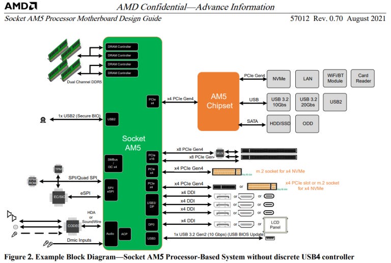
AM5 now features an additional 4x PCIe Gen 4 lanes, which might be useful for attaching more M.2 slots or implementing a a discrete USB4 controller. These extra PCIe lanes won’t be available with all AM5 CPUs though (see table below). Unlike with Genoa, there’s no mention of PCIe 5 support on AM5 CPUs. AMD seems to have chosen more lanes instead of faster lanes.
USB BIOS update capability is built in, and provided on a 10 Gbps USB port. Combined with MPIO in Genoa, there seems to be a trend of AMD taking over functionality traditionally handled by motherboard manufacturers. This particular move is very understandable considering that AMD kept the same AM4 socket across several generations, but AM4 forward compatibility was often far from straightforward. Because built in USB flashing was far from universal, AMD provided short term CPU loans so people could flash their BIOS to support new processors.
AM5 will make that a thing of the past. AMD’s motherboard design guide states that the “USB BIOS Update feature is integrated into all AM5 processors” and is activated when a GPIO pin (AGPIO23) is asserted at power on. AMD recommends that boards implement a button connected to AGPIO23. I personally hope that board makers will take this advice instead of doing something stupid like asking users to short two inconveniently placed pins with a screwdriver.
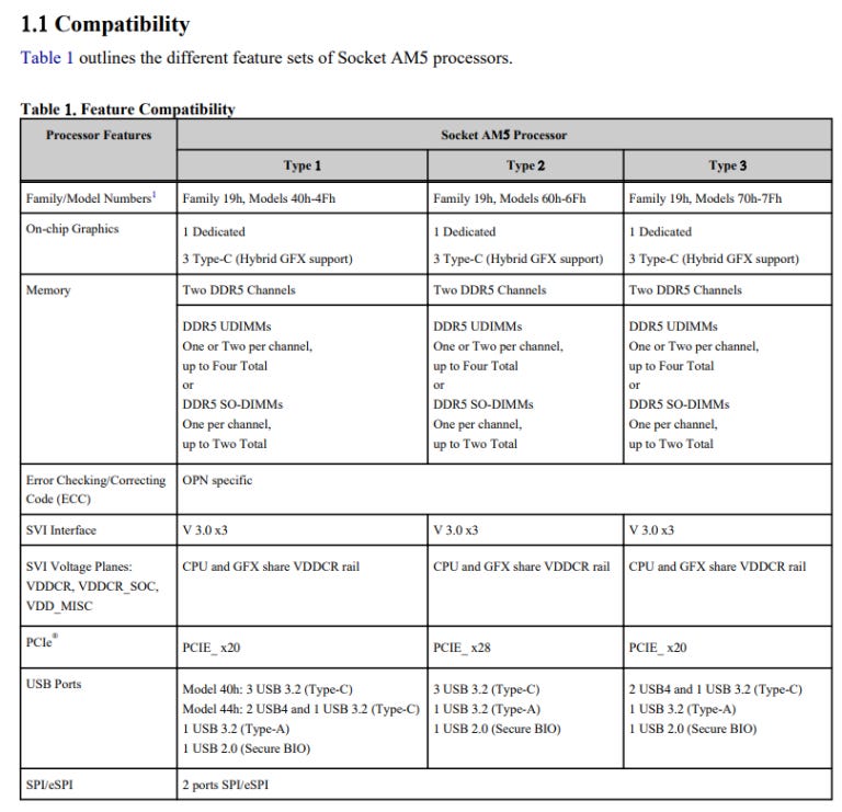
iGPUs may also make an appearance on more AM5 CPUs. On-chip graphics are mentioned for all three types of AM5 processors. A note at the bottom says “Some OPNs…may not support GFX”, but AMD’s approach with iGPUs seems to be converging with Intel’s – all three types are referred to as APUs elsewhere in the document. Thus AM5 CPUs without iGPUs may just be chips with a defective/disabled iGPU.
There are probably some users who want the processing power of AMD’s CPUs without having to buy a discrete GPU. In conjunction with the BIOS update feature, integrated graphics make a lot of sense (making it easier to set up or troubleshoot a system).
Display output for the iGPU is also quite flexible. Four DisplayPort interfaces are provided from the CPU, and three of them can be routed to USB-C ports in DP Alt Mode. I couldn’t find DisplayPort versions, but AMD provides schematics for converting the DisplayPort signal to HDMI 2.1 so there should be enough bandwidth to drive a 4K60 display.
Closing Comments
Obviously, both the client and server variants of Zen 4 are quite far out. But this early glimpse of Zen 4 shows a core architecture with a lot of similarities to Zen 3, and a repeat of the Zen 1 to Zen 2 transition is a distinct possibility.
For the core, moving to TSMC 5nm comes with effort and risk. Avoiding sweeping microarchitecture changes at the same time is a pretty solid strategy. Beefing up the DTLBs and L2 cache should offer reasonable IPC gains on their own. AMD will certainly increase the size of other core structures too. And AVX-512 support will bring huge gains in applications that support it.
Outside the core, the AM5 client platform evolves to support DDR5 and provide more PCIe lanes from the CPU, along with quality-of-life improvements. Genoa sees major changes with 12 DDR5 channels, increased core count, PCIe 5, and support for larger, scale out memory solutions. In that respect, the server platform’s changes are similar to the Zen 1 to Zen 2 transition too. AMD is using a new process technology to increase core counts, while making substantial IO changes.