FuriosaAI’s RNGD at Hot Chips 2024: Accelerating AI with a More Flexible Primitive
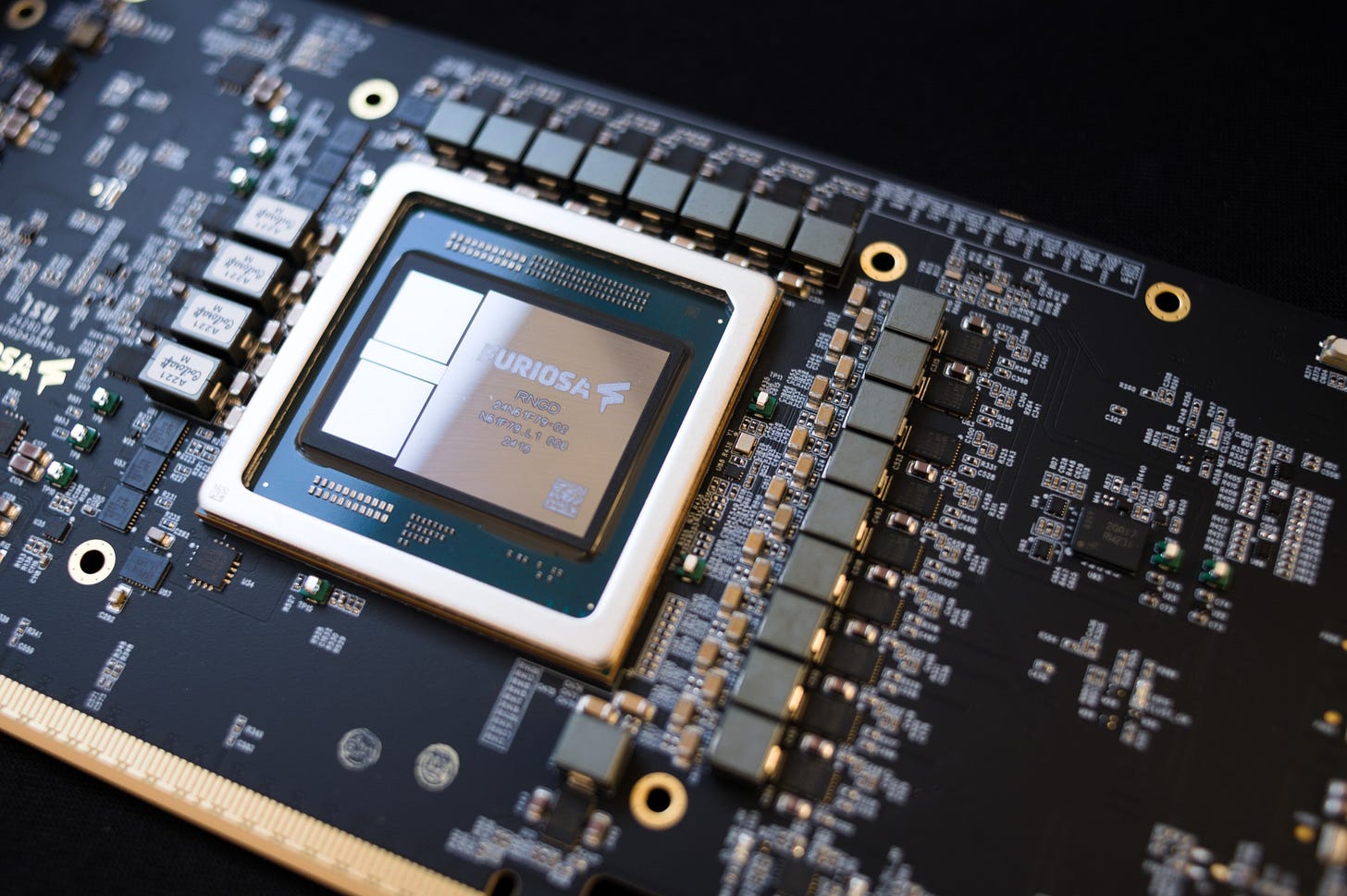
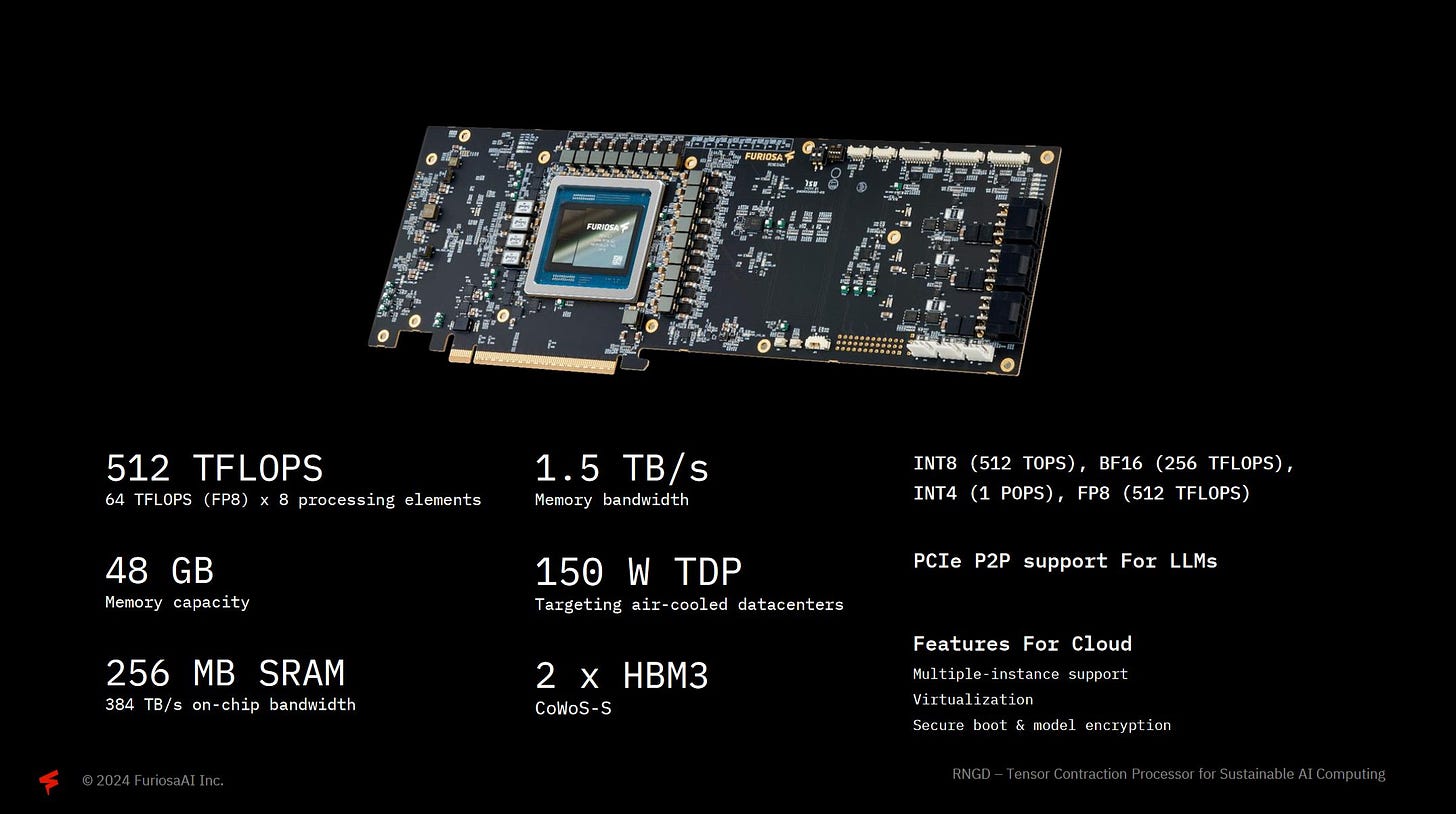
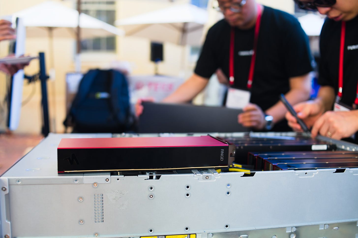
There were no shortage of AI accelerators at Hot Chips 2024. One of those was FuriosaAI’s RNGD, pronounced Renegade. It’s a 150W TDP chip with 48 GB of HBM3, and aims to handle inference at lower power than GPUs. RNGD is physically implemented on a PCIe card, and is used as an accelerator much like a GPU. However, FuriosaAI aims for better power efficiency than a GPU with their custom architecture.
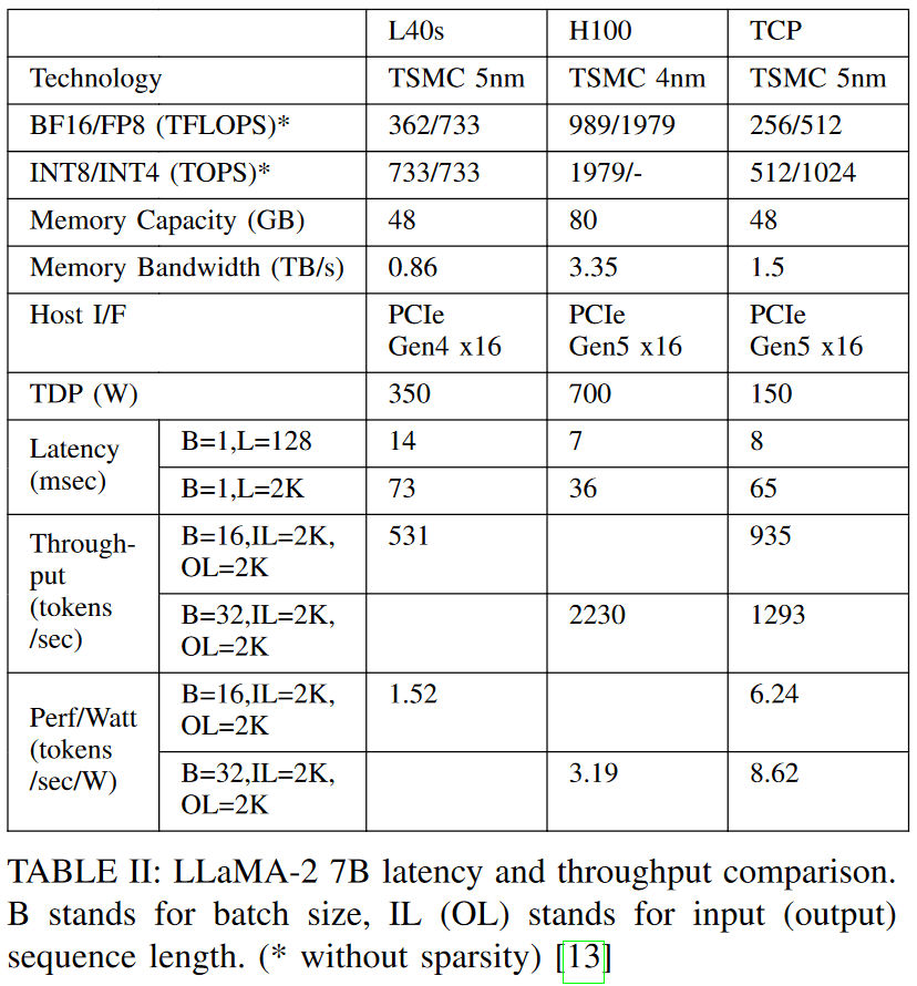
RNGD has a high compute to memory bandwidth ratio. The card’s TDP is a conservative 150W, well below the 350W power target of Nvidia’s H100 PCIe. FuriosaAI wants to make RNGD easy to install in existing air cooled datacenters, and keeping power draw low helps achieve that goal.
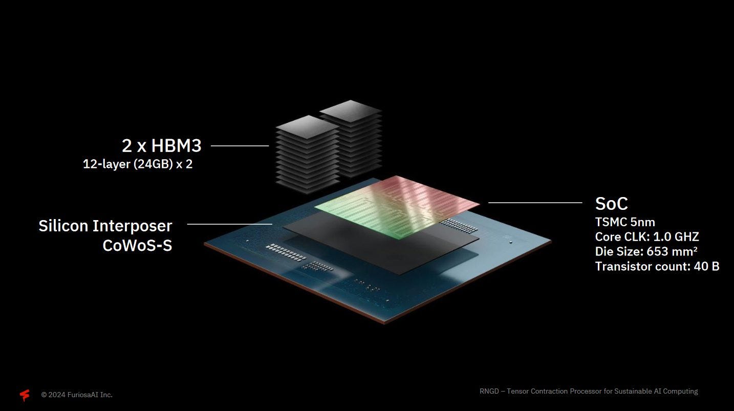
Low power is achieved using TSMC’s 5 nm process, and running a large array of execution units at a very conservative 1 GHz. RNGD uses 2.5D packaging, with HBM modules and SoC integrated on a single interposer. They’re using the newest 12-layer HBM3 to maximize memory capacity and efficiency.
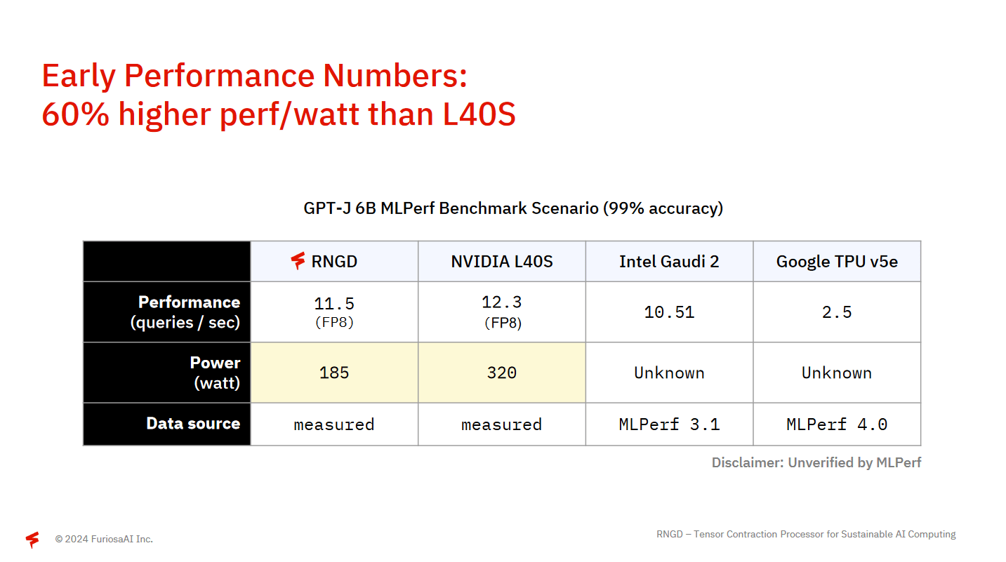
FuriosaAI has chosen MLPerf to show off their power efficiency. While GPT-J is not the most recent model, they believe performance optimizations applied to GPT-J are generally applicable to other language models.
In speed terms, RNGD is processing about 1000 tokens per second and delivers about 40% more performance per watt than Nvidia’s L40S. FuriosaAI is also proud that they were able to achieve this level of performance and power efficiency just three months after getting silicon back from the foundry. Therefore, they believe there’s substantial room for further improvement in the coming months.
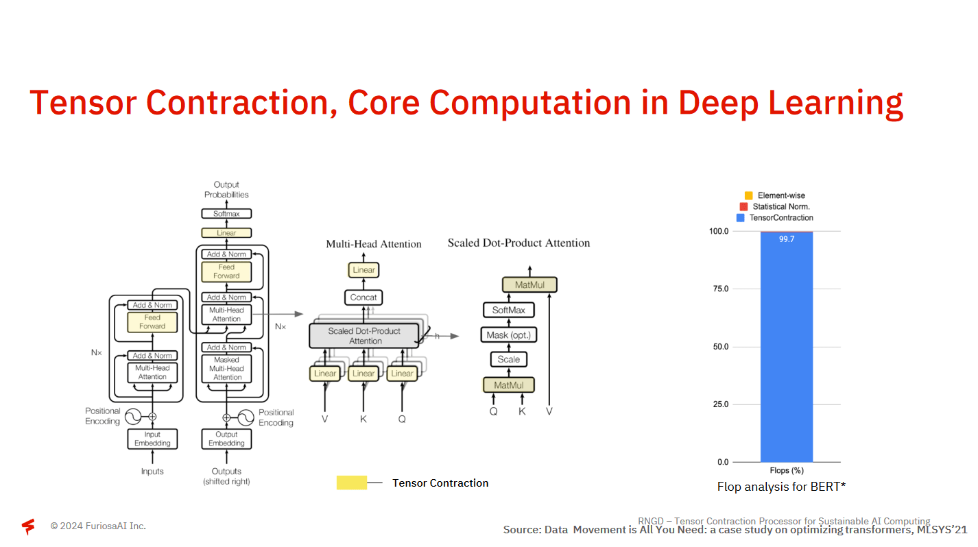
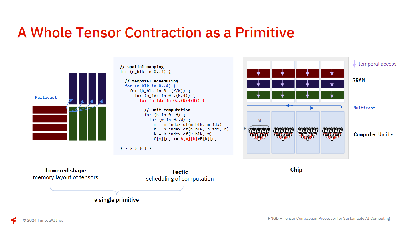
Another reason they believe there’s room for further improvement is that RNGD is built to be more flexible than other AI accelerators. RNGD uses tensor contraction as a primitive operation, rather than matrix multiplication as in Google’s TPU or GPUs. Tensor contraction is a more general operation that includes matrix multiplication. FuriosaAI believes generalizing the hardware a bit gives them more room to benefit from future software optimizations.
For comparison, Nvidia’s tensor cores use fixed-size matrix multiplication as a primitive operation, as do AMD GPUs with WMMA/MFMA instructions. An easier way of thinking about it is, RNGD’s tensor units accelerate dot product and accumulate operations. Optimization opportunities come from scheduling computations within a tensor contraction operation to maximize data reuse, and keeping “hot” data in on-chip SRAM. FuriosaAI also noted that large matrix multiplication units, like the 128×128 ones in Google’s TPU, can be hard to utilize with varying batch sizes often encountered with inference.
Hot Chips 2024 mostly focuses on hardware architecture. In the spirit of Hot Chips, I’m going to deviate from the presentation at this point to go over RNGD’s architecture. Much of that is detailed in FuriosaAI’s paper, so I’ll be discussing details from both the presentation and the paper here.
Hardware Architecture
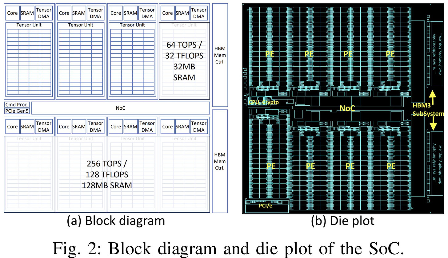
RNGD is built from Processing Elements (PEs), which behave as independent AI cores. A PE can function independently, or be fused in a set of up to four PEs to act as a single large processing element.
The PE has a CPU core for scalar processing and control flow. The CPU core has a minimal cache hierarchy with 64 KB of instruction and data caches, probably arranged as a 32 KB instruction cache and 32 KB data cache. There’s also a 256 KB L2. CPU code runs completely out of a 3.5 MB block of SRAM memory, insulating the core from DRAM. A Tensor DMA unit sits alongside the CPU core, and helps move data into the PE’s Tensor Unit. Ideally, the Tensor DMA unit handle data movement while the Tensor Units perform computation.
Most of RNGD’s throughput is focused in Tensor Units (TUs), which are further subdivided into 64 Slices. A TU physically has 65 Slices, but one is a spare to improve yields. RNGD’s Slices are reminiscent of AIE tiles in AMD’s NPU. Both are arranged on a fetch network, with a multicast mechanism that allows broadcasting data read from one Slice’s SRAM to other Slices that need it.
To the PE’s CPU core, the TU is a coprocessor with a large set of control registers. Besides control registers, the TU also has a command processor, a bit like a GPU. The PE’s CPU core pushes commands to the command processor through a 64 entry queue. That lets the TU perform certain operations asynchronously, without needing the PE CPU to directly set all the necessary control registers. As with a GPU, command execution can overlap, and the PE CPU must add wait commands to ensure proper ordering.
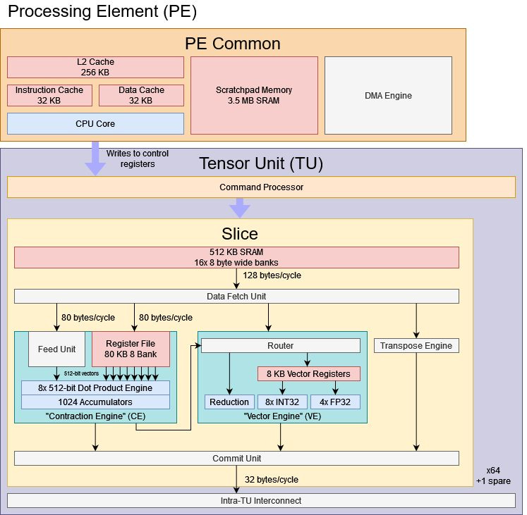
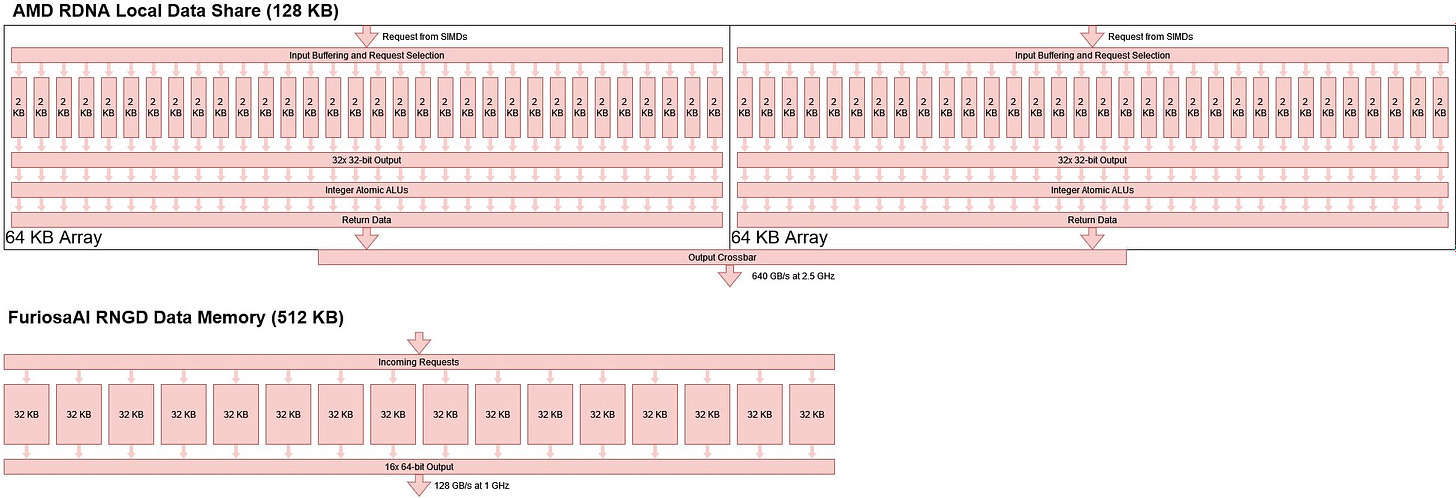
Each of the TU’s Slices has 512 KB of SRAM, for 32 MB of SRAM capacity across the TU. Each SRAM block is built from 16x 32 KB banks, each 8B wide. That’s good for 128 GB/s of bandwidth at 1 GHz. Banking lets the SRAM block service multiple accesses simultaneously, like writing data streamed in from HBM memory to SRAM while reading out data to feed the execution units. Curiously, the SRAM block supports virtual addressing. Thus while it’s not a cache, this SRAM block is more flexible than the local memory blocks found on GPUs.
One comparison is the Local Data Share blocks in AMD’s RDNA GPU architecture. RDNA’s LDS has 128 KB of capacity and is built from 64x 2 KB banks, each 32 bits (4 bytes) wide. A RDNA LDS instance can provide twice as much per-cycle bandwidth as a RNGD SRAM slice, and that difference gets even larger when you consider RDNA’s higher clock speeds. Finer banking also gives RDNA’s LDS more flexibility to handle different access patterns.
But RNGD’s Slice SRAM is well suited to its purpose. Lower bandwidth is less of an issue because machine learning involves a lot of redundant reads, and multicasting a read can amplify bandwidth. For example, matrix multiplication involves taking the dot product of a row in one matrix with many columns in another. A row read can be broadcast, saving bandwidth. Fewer banks matter less because AI memory access patterns are more predictable, and largely linear.
Predictability is likely why RNGD’s SRAM slices are optimized for capacity, and that’s where RNGD really excels. AMD’s RX 6900 XT only has 5 MB of LDS across the GPU, and relies on a 128 MB last level cache to alleviate memory bandwidth bottlenecks. RNGD has 32 MB of SRAM in each TU, for 256 MB across the chip. Plain SRAM blocks don’t need tag and state arrays, making them less power and area hungry than caches. Caches can flexibly adapt to different access patterns in various applications, but a specialized machine learning accelerator doesn’t try to do that.
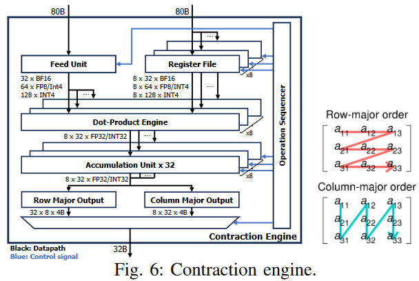
A Slice’s compute power is concentrated in the Contraction Engine (CE), which has a set of dot product units and accumulators. Specifically, there are eight dot product units. Each takes a pair of 512-bit input vectors and then outputs the dot product. The dot product units can be fed from data coming off the intra-TU interconnect, or a 80 KB register file. Much like in GPUs, the register file is constructed with single port SRAM banks. GPUs typically have four SRAM banks, but RNGD uses eight register banks to match the number of dot product engines. Furiosa also has a small register cache of unknown size for frequently reused operands. Dot product results are fed into a set of 1024 accumulators.
Matrix multiplication boils down to doing dot products, so the CE’s architecture should still be very efficient with matrix multiplication. The 512-bit vector length corresponds to 32 BF16 or 64 FP8 elements, so the CE operates on a smaller granule of data than the 128×128 matrix multiplication units of Google’s TPU. However, GPUs do operate on smaller matrices. RDNA 3’s WMMA instructions operate on 16×16 matrices for example.
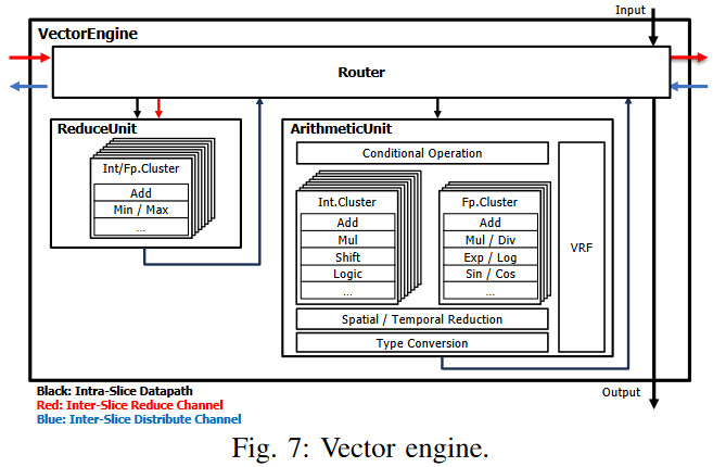
A Vector Engine (VE) sits alongside the Contraction Engine. While the CE provides a lot of throughput, it’s limited to lower precision INT4/8, FP8, and BF16 data types. The VE can handle FP32 and INT32 as well as lower precision types. The VE can handle higher precision, though at smaller 256-bit or 128-bit vector lengths. It’s fed by a 8 KB register file. While small compared to the CE’s 80 KB register file, it’s comparable to vector register file sizes on CPUs. For example, Zen 4 and Zen 2 have 12 KB and 5 KB of vector register file capacity, respectively. SHAVE DSPs on Intel’s NPU are vaguely comparable to RNGD’s VE. Both use modest vector lengths, handle data types not supported on the wider dot product or matrix multiplication units, and can perform transcendental operations.
Besides the CE and VE, each Slice has a Transpose Engine (TE) for rearranging data. All three units can operate simultaneously. Results from those units head to a Commit Unit, which can write out up to 32 bytes per cycle. Smaller 8 byte and 16 byte commit sizes are supported too. The Commit Unit can also do type conversions.
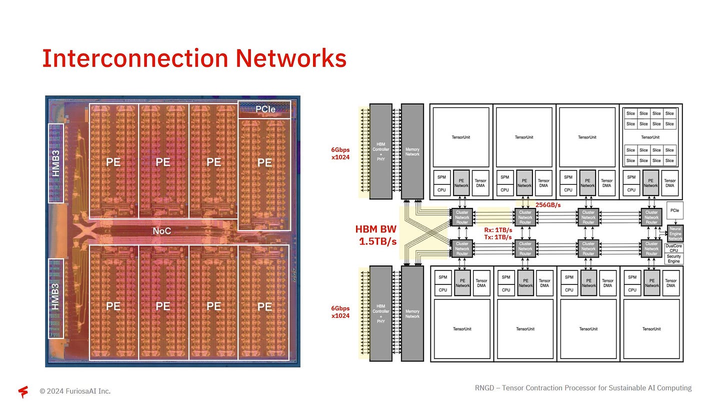
PEs are connected to the rest of the system via a high bandwidth on-chip network. FuriosaAI’s slide shows the interconnect’s layout, and suggests each cluster network router has a 1024 byte/cycle link to its left/right neighbors. It’s a much wider link than the 32B/cycle or 64B/cycle ones on client ring buses, showing how bandwidth hungry FuriosaAI expects ML workloads to be.
RNGD has 16 HBM channels, and its interconnect can give any PE access to full HBM bandwidth. The two HBM3 stacks on RNGD can provide 1.5 TB/s of bandwidth. While higher than bandwidth on client GPUs, Nvidia’s H100 and AMD’s MI300X use more HBM stacks for even more bandwidth.
Host communication goes through a PCIe 5 x16 interface, which is also used for peer-to-peer communication. Data passed between RNGD cards on the same system can go through a PCIe switch without consuming upstream host resources. A server can have up to 20 RNGD chips for large models, with the model partitioned across multiple chips.
AMD and Nvidia in contrast use custom links to provide higher bandwidth between peer GPUs. AMD’s MI300X has seven Infinity Fabric links for 896 GB/s of off-chip bandwidth. Nvidia’s H100 has 18 NVLink links for 900 GB/s of bandwidth to peer GPUs.
Final Words
FuriosaAI’s RNGD tries to be more flexible than other accelerators, which makes it an interesting product to talk about. But RNGD has limitations. FuriosaAI is using top shelf HBM3 memory, but two stacks can only give them 48 GB of memory capacity. Nvidia’s H100 has 80 GB of memory, and AMD’s MI300X has a whopping 192 GB. For models that can’t fit on one card, Nvidia and AMD have very high speed cross-GPU links. RNGD uses plain PCIe 5.0 x16 links. That could give RNGD a hard time with larger models that need higher memory capacity. I’m sure software optimizations will help RNGD down the road, but I have a feeling getting around DRAM capacity limits without a lot of cross-card bandwidth will be difficult.

Where RNGD really shines is its low power consumption. Personally, I love seeing that 150W power target. It reminds me of GPUs in the Nvidia Maxwell and Pascal era, where I could expect decent gaming performance without blowing 200W. GPUs today are far more power hungry, and that’s even more the case with big compute GPUs like AMD’s MI300X or Nvidia’s H100.
If you’re a financial analyst, this is the last sentence in the article. But if you’re not, RNGD may also have a price advantage. FuriosaAI hasn’t set prices for RNGD cards. But in side conversations with FuriosaAI folks, RNGD’s price will likely be around $10k. That makes it cheaper than AMD’s MI300X, which Tom’s Hardware believes costs $10K-$15k, and much cheaper than the $40k H100. It’s not hard to see why. More HBM stacks and custom high bandwidth interconnects are expensive. RNGD is light on both of those. Hopefully those won’t limit its ability to adapt to changes in the AI landscape, especially as models seem to get ever larger.
If you like our articles and journalism, and you want to support us in our endeavors, then consider heading over to our Patreon or our PayPal if you want to toss a few bucks our way. If you would like to talk with the Chips and Cheese staff and the people behind the scenes, then consider joining our Discord.


