Telum II at Hot Chips 2024: Mainframe with a Unique Caching Strategy
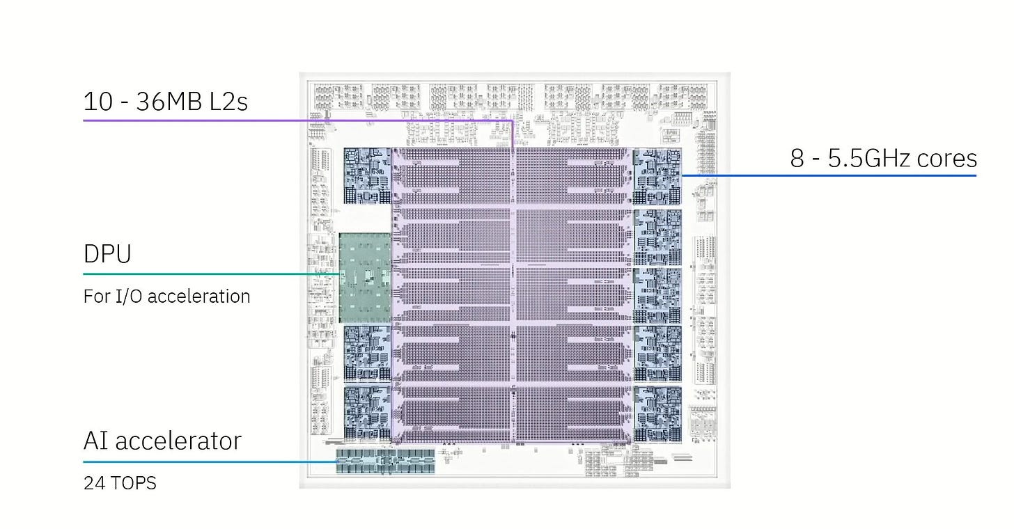
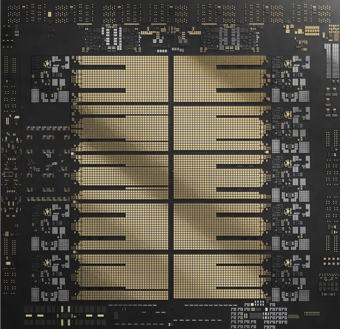
Mainframes still play a vital role in today, providing extremely high uptime and low latency for financial transactions. Telum II is IBM’s latest mainframe processor, and is designed unlike any other server CPU. It only has eight cores, but runs them at a very high 5.5 GHz and feeds them with 360 MB of on-chip cache. IBM also includes a DPU for accelerating IO, along with an on-board AI accelerator. Telum II is implemented on Samsung’s leading edge 5 nm process node.
IBM’s presentation has already been covered by other outlets. Therefore I’ll focus on what I feel like is Telum (II)’s most interesting features. DRAM latency and bandwidth limitations often mean good caching is critical to performance, and IBM has a often deployed interesting caching solutions. Telum II is no exception, carrying forward a virtual L3 and virtual L4 strategy from prior IBM chips.
Virtual L3
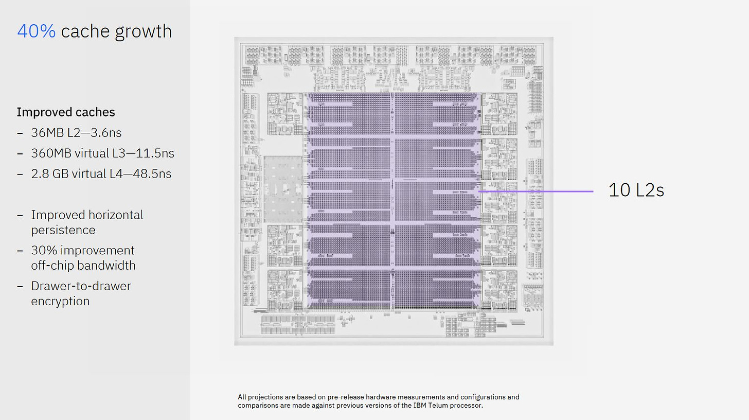
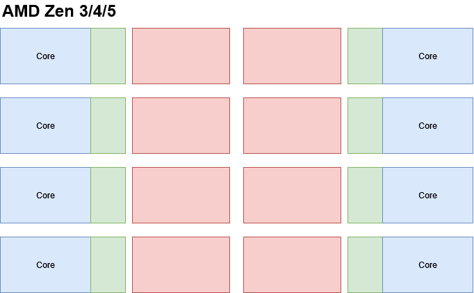
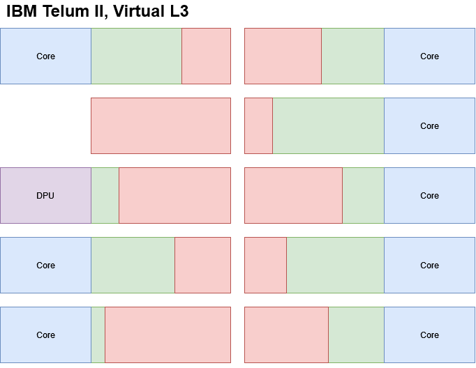
Telum II has ten 36 MB L2 on-chip, which is absolutely huge. For perspective, the L3 cache on AMD’s Zen 3 desktop and server CPUs is typically 32 MB. Eight of Telum II’s L2 caches areare attached to cores, another is attached to the DPU, and a final tenth one isn’t attached to anything. Another comparison is Qualcomm’s Oryon core in the Snapdragon X Elite, which has a 12 MB L2 cache with 5.29 ns of latency. Qualcomm considers a tightly coupled high capacity cache. Telum II has 3.6 ns of L2 latency, and more capacity to boot.
These giant L2s are great for cutting down memory access latency, but put Telum II in a funny position. Modern CPUs typically have a large cache shared across multiple cores. A shared cache can give a single thread more capacity in low-threaded loads, and reduce duplication for shared data in multithreaded loads. But eight cores in Telum II would already use 288 MB of SRAM capacity, along with the associated area and power cost. An even larger L3 would be expensive even for a specialized mainframe chip.
IBM’s solution is to reduce data duplication within its caches, and re-use the chip’s massive L2 capacity to create a virtual L3 cache. From IBM’s patent, each L2 has a “Saturation Metric” based on how often its core brings data into it (to satisfy misses). When a L2 kicks out a cache line to make room for incoming data, that evicted line goes another L2 with a lower Saturation Metric. That way, a core already pushing the limits of its own L2 capacity can keep that capacity to itself. The L2 slice without an attached core always has the lowest possible Saturation Metric, making it a preferred destination for lines evicted out of L2. If another L2 already has a copy if the evicted line, Telum II gives that L2 ownership of the line instead of putting it into virtual L3, also reducing data duplication.
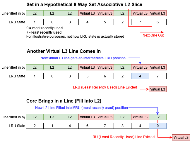
Tracking Saturation Metrics isn’t the only way IBM keeps the virtual L3 from monopolizing L2 capacity. IBM’s patent also mentions inserting virtual L3 lines into intermediate LRU positions. Replacement strategy is how a cache chooses a line to kick out when a new line is brought in. LRU stands for Least Recently Used, and is a replacement policy where the least recently used line gets kicked out. Normally, a newly inserted line gets put into the MRU (most recently used) position, putting it last in line to get replaced. But virtual L3 lines can get put into intermediate positions, giving priority to L2 lines brought in by the core.
Using intermediate positions also lets IBM control how much L2 capacity the virtual L3 can use. For example, putting virtual L3 fills halfway between the LRU and MRU positions would limit the virtual L3 to using half of L2 capacity. It’s easy to see how IBM can use this to elegantly adapt to changing application demands. If one core goes idle, its L2 could start inserting virtual L3 fills at the LRU position, letting the virtual L3 use all available capacity in that slice.
Besides making L2 capacity doesn’t get squished out, the virtual L3 faces another challenge. A line in the virtual L3 could be in any of Telum II’s ten L2 slices. In AMD, Arm, and Intel’s L3 caches, an address always goes to the same slice. A core can look at a subset of an address’s bits, and knows exactly which L3 slice to send a request to. That’s not the case for IBM. Apparently IBM handles this by potentially checking all L2 slices for a virtual L3 access. I asked if they were worried about overhead from more tag comparisons, but they said it wasn’t an issue because L2 miss rate was low. It’s important to remember that engineers try to keep a CPU design balanced, rather than pouring resources into making sure it’s great at every last thing. A Telum II core can use up to 36 MB of L2 capacity. Other factors being equal, it should miss L2 less often than a Zen 5 core misses in its 32 MB L3. A L3 access on Zen 5 may cost less power, but AMD needs that to be the case because Zen 5 cores have an order of magnitude less L2 capacity than Telum II’s cores.
Why Stop at L3?
IBM’s mainframe chips aren’t deployed in isolation. Up to 32 Telum II processors can be connected to form a large shared memory system. Again, IBM is looking at a lot of cache capacity, this time across a system instead of a single Telum II chip. And again, they applied the same virtual cache concept. Telum II creates a 2.8 GB virtual L4 by sending L3 victims to other Telum II chips with spare cache capacity.
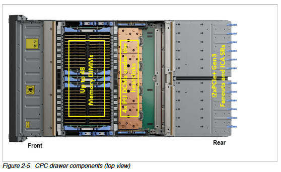
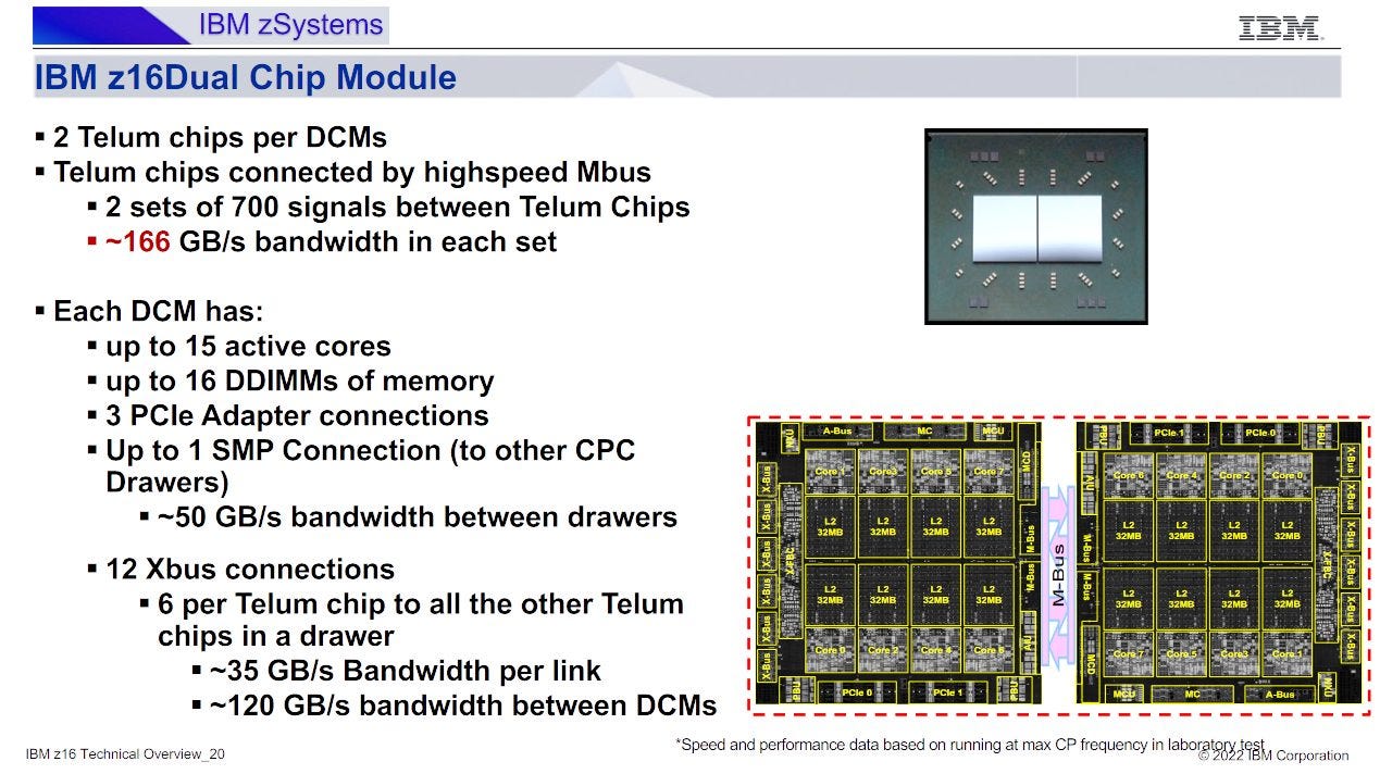
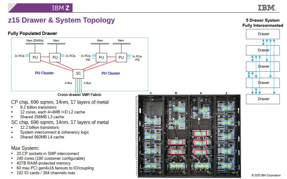
I’m not sure how IBM implemented the virtual L4, but prior IBM mainframe designs might provide some clues. IBM organizes mainframe CPUs into CPC drawers, which somewhat resemble a rack-mount servers. A CPC can’t operate independently like a server because it doesn’t include non-volatile storage or a power supply unit, but it does place a set of CPUs and DRAM in close physical proximity. Prior IBM designs had a drawer-wide L4, and Telum II might do the same. 2.8 GB of L4 aligns with on-chip cache capacity across eight Telum II chips. If a drawer has eight Telum II dies, just as a Z16 drawer had eight Telum dies, then IBM could be persisting L3 victims across a drawer.
IBM claims 48.5 ns of latency for a virtual L4 access. Achieving that across drawer boundaries would be quite a challenge. As ambitious as Telum II is, I think that would be a bridge too far. On the latency subject, IBM’s likely betting that L3 misses are rare enough that 48.5 ns of L4 latency isn’t a big deal. IBM also deserves a lot of credit for getting latency to be so low when crossing die boundaries. For perspective, Nvidia’s Grace superchip has over 42 ns of L3 latency with a monolithic die.
Looking Back at Telum
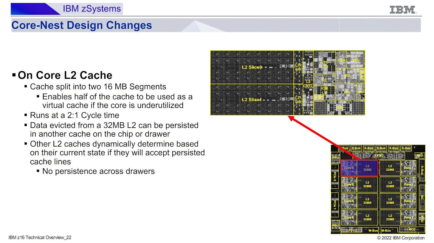
When talking about Telum II’s caching strategy, it’s impossible to ignore the original Telum/Z16. That’s where IBM brought virtual L3 and L4 caches into their mainframe line. Telum was presented at last year’s Hot Chips 2023. Since then, IBM has published more info on how Telum’s virtual L3/L4 setup worked. It’s a fairly simple scheme where each 32 MB L2 slice is split into two 16 MB segments. One segments can become part of the virtual L3/L4 if a core doesn’t need all of its L2 capacity. If the core is idle, all 32 MB can go towards the virtual L3/L4.
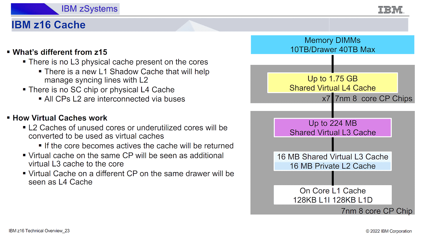
IBM’s technical overview furthermore clarifies that the virtual L4 is implemented across a drawer. A Z16 drawer has eight Telum chips, each with 256 MB of L2 capacity. A single threaded workload running on a drawer gets its own 32 MB L2. All the other on-die L2 caches become that thread’s 224 MB L3, and other L2 caches within the drawer combine to form a 1.75 GB virtual L4.
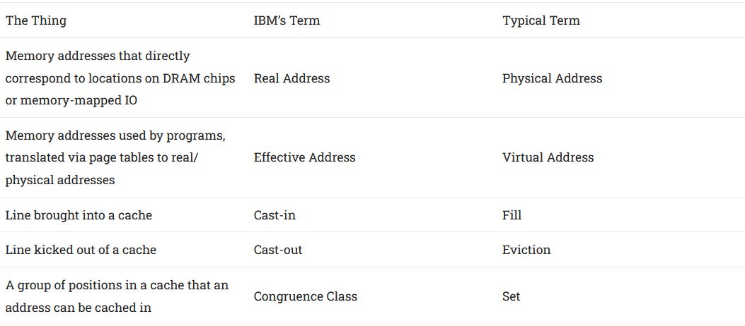
Telum II takes that strategy further, with higher cache capacity at L2, virtual L3, and virtual L4. When I asked how Telum II handled its virtual L3 after Cheese did his interview, they mentioned congruence classes. I had no clue what a congruence class was. IBM after all uses different terminology that I wasn’t familiar with, and it took quite some searching to figure out that a congruence class was basically a cache set.
Funny enough, I asked why IBM had different terminology compared to the rest of the industry. They said IBM came up with the terminology first, and later on the industry adopted different terminology. It was all lighthearted and funny. But it’s also a reminder that IBM was a pioneering company in developing high performance CPUs.
Final Words
CPU designers have to strike a balance between single and multithreaded performance. Server CPUs tend to focus on the latter, while client designs do the opposite. Telum II and prior IBM mainframe chips handle server tasks like financial transactions, but curiously seem to prioritize single threaded performance. IBM has actually decreased core counts per die from 12 in Z15 to 8 in Telum and Telum II. The focus on single threaded performance is very visible in IBM’s caching strategy as well. A single thread running on Telum II can enjoy client-like L2 and L3 access latencies, but with an order of magnitude more capacity at each level.
I wonder if IBM’s strategies can be applicable to client designs. AMD’s highest end CPUs notably have a lot of L3 cache capacity on the chip. For example, the Ryzen 9 9950X has 32 MB of L3 and 8 MB of L2 per CCD. Both CCDs together would give 64 MB of L3 and 16 MB of L2, for 80 MB of total caching capacity. If all that could be used for a single thread, it’s not far off from the 96 MB of L3 cache that a VCache part gets. A hypothetical dual CCD part with VCache on both dies could have over 200 MB of virtual L3 capacity.
Of course, pulling that off isn’t so straightforward. IBM’s mainframe chips use very fast cross-die interconnects. A Zen 5 CCD’s Infinity Fabric link only provides 64 GB/s and 32 GB/s of read and write bandwidth, respectively. IBM’s prior generation Telum already has twice as much bandwidth between dual-chip modules, and even more than that between Telum chips located on the same module.
Perhaps AMD calculated that consumers weren’t willing the pay the premium for advanced packaging technologies in client CPUs. But I do wonder what would happen if AMD could be the Nvidia of the GPU market, where enthusiasts don’t object to paying over $2000 for a top end SKU. Games tend to be cache sensitive, as VCache has shown. Perhaps such a part with a CoWoS-R RDL interposer or a similar packaging technology and a virtual L3 could push gaming performance even further.
I’d like to thank IBM for giving an excellent presentation at Hot Chips 2024, as well as discussing parts of their architecture in side conversations.
If you like our articles and journalism, and you want to support us in our endeavors, then consider heading over to our Patreon or our PayPal if you want to toss a few bucks our way. If you would like to talk with the Chips and Cheese staff and the people behind the scenes, then consider joining our Discord.


