
Tracing Intel’s Atom Journey: Goldmont Plus

Today Intel’s Atom line occupies a prominent place in Intel’s best client chips. Atom cores are also going into Intel’s upcoming Sierra Forest server CPU, where they’ll similarly aim to deliver area efficient multithreaded performance. But a few generations ago, Intel’s Atoms were stuck in low power devices where they were nearly forgotten as people focused on Intel’s high performance cores.

Here, I’ll look at Goldmont Plus, an architecture from Atom’s darker days. Goldmont Plus launched in late 2017 on Intel’s 14 nm node, and was discontinued in 2020. Even though Goldmont Plus didn’t have a clear market segment where it could dominate, it’s an interesting step in Atom’s evolution. Older Atoms like Silvermont targeted cell phones on older process nodes, which meant heavy compromises to cope with tight power constraints. Tremont came after, and represents a huge step up likely because Intel was revving up their hybrid core strategy. Goldmont Plus sits between those two extremes.
I’ll be testing the Celeron J4125, which implements a quad core Goldmont Plus cluster with 4 MB of L2 cache in a FCBGA1090 package. CPU clock speeds can boost up to 2.7 GHz. While the Celeron J4125 targets 10W, power consumption can often reach 13-14W under all core loads.
Overview
Goldmont Plus (GLP) is a 3-wide superscalar, out-of-order architecture. Its execution engine is wider and has much more reordering capacity than early Atoms like Silvermont. In some respects, it’s comparable to Intel’s Core 2 architecture. But unlike recent Atoms like Crestmont and Skymont, Goldmont Plus doesn’t get close to big cores that came a few generations before it.

Like modern Atoms though, Goldmont Plus shares traits like a distributed scheduler and predecode mechanism. Intel says GLP has a 12-13 cycle branch mispredict penalty, which is shorter than 15-20 cycle mispredict penalty in Intel’s higher performance cores.
Frontend: Branch Prediction
Accurate branch prediction is important for both performance and power efficiency, but designers have to balance the branch predictor’s area and power usage with the benefits of better prediction. Earlier Atoms like Silvermont (in the Knights Landing variant) had a weak branch predictor, and so did many low power cores from the early to mid 2010s. Arm’s Cortex A73 has similar characteristics. Goldmont Plus abandons the cell phone form factor, likely giving it the power and area budget necessary for a more sophisticated branch predictor. Its pattern recognition capabilities feel more like Skylake’s, though it doesn’t do quite as well with large branch footprints.

Branch target caching takes a cut too. Goldmont Plus has a 2048 entry BTB with 3 cycle latency. Capacity matches Intel’s older Nehalem and Core 2, though speed is quite poor in comparison. Core 2 for example has 2 cycle BTB latency, and can handle up to four branches with single cycle latency.

Since then, branch target caching has gone bigger and faster on Intel’s big cores. Haswell can track 128 taken branches with single cycle latency, while retaining 2 cycle latency on a 4096 entry main BTB. Modern Atoms like Crestmont also have strong branch target caching.

Branch target caching gets harder with indirect branches, which can go to many different targets. GLP can track at least 128 indirect targets with little penalty, with 32 indirect branches each cycling between four targets. A single indirect branch can cycle between 16 different targets before taking substantial penalties.

While GLP’s indirect prediction capabilities aren’t as good as big cores, a basic indirect predictor is better than nothing.
Frontend: Fetch and Decode
After the branch predictor decides where to go, the frontend grabs instructions from those specified memory locations and translates them into the CPU’s internal format. Goldmont Plus has a 32 KB instruction cache, and has a 64 KB predecode cache alongside it to simplify the main decoders. Unlike the predecode setup in Arm’s cores, where predecode info is tied to the instruction cache, Goldmont Plus’s separate predecode cache lets it keep predecode info for instructions even after they’re evicted from L1. That lets the CPU avoid re-doing the predecode process for larger instruction footprints. A 48 entry fully associative instruction TLB helps speed up address translations in the frontend.

According to Intel’s optimization guide, the decoders can handle 20 bytes per cycle. However, I could only sustain 16 bytes per cycle using 8B NOPs. Intel’s higher performance cores have a micro-op cache that bypasses instruction cache bandwidth limits, which can help code with lots of immediate values or AVX instructions with extra prefixes.
Goldmont Plus’ decoders can handle up to three instructions per cycle, matching contemporary low power CPUs like Arm’s Cortex A72. It falls short of Intel high performance cores, which can decode four instructions per cycle. But stopping at 3-wide is a good decision when throughput is likely to be limited by other reasons like cache latency.

If code spills out of L1i, Goldmont Plus maintains good instruction throughput for a low power core, likely because the predecode cache allows for faster L1i fills. Cortex A72 is also 3-wide but loses a lot of throughput if it has to run code from L2. A72 might have weak predecoders, or can’t generate enough instruction-side memory level parallelism to hide L2 latency.
Rename and Allocate
After instructions are fetched and decoded, the rename/allocate stage has to give it backend resources so it can be tracked for out-of-order execution. That involves renaming registers from ISA ones to internal ones, breaking false write-after-write dependencies in the process and allowing more instruction level parallelism. Besides register renaming, this stage can pull various tricks to further boost parallelism.

Goldmont Plus recognizes the most common zeroing idioms and can sometimes perform move elimination. It somewhat resembles Skylake in that respect.
Uniquely, Goldmont Plus has a wider rename stage than its frontend. The renamer can deal with four micro-ops per cycle, while the frontend can only deliver three per cycle. I’m not sure why Intel did this. Perhaps they were setting the stage for Tremont, which similarly has 4-wide renamer but packs a frontend wide enough to feed it.
Out-of-Order Execution
Intel’s earlier Silvermont architecture used an ROB-based scheme, with speculative register files large enough to cover the entire ROB and a separate architectural register file to store known-good results. That scheme is simpler to handle because registers don’t have to be tracked independently of ROB entries, but causes more data movement because register values have to be copied into the retired register file as instructions retire (complete). Goldmont Plus switches to a modern PRF (physical register file) scheme where the ROB stores pointers to register file entries, and the PRF stores both speculative and known-good results.

However, that means the backend can be unable to receive incoming operations if it runs out of PRF entries. Goldmont Plus’ integer and floating point register files appear to have 66 and 75 entries available for renaming, respectively. That’s enough to cover most of the reorder buffer in most cases, because every program will have instructions that don’t need a register file entry. Stores and jumps come to mind.
Assuming register files aren’t a limitation, GLP’s 93 entry ROB provides similar reordering capacity to Intel’s Core 2. It falls quite short of newer Intel architectures like Sandy Bridge and Haswell, which have 168 and 192 entry ROBs respectively. But it is a good step up from Silvermont’s 32 entry ROB.
Scheduling and Execution
Goldmont Plus uses a distributed integer scheduler like other Atoms. The most common ALU instructions have a decent 30 scheduling entries available, representing a large boost over Silvermont. Branches go to a separate port with eight scheduler entries, reducing pressure on the ALU ports. The dedicated branch port also naturally prioritizes branches because they won’t experience contention with other ALU operations. That in turn helps detect mispredicted branches faster and reduce wasted work.

High performance cores like AMD’s Zen have more integer execution resources and larger schedulers, making them better at finding instruction level parallelism.
Low power cores like Goldmont Plus usually have have to sacrifice floating point and vector execution. There are only two FP pipes, specialized to perform floating point adds and multiplies. Vector integer operations can go down either pipe, likely because integer ALUs cost less power and area than floating point units. Both pipes have 128-bit execution units, since Goldmont Plus doesn’t support AVX. Compared to Silvermont, GLP does benefit from a larger, unified FP scheduler. That should help it absorb FP execution latency.

AMD’s Zen architecture also has 128-bit execution units, but splits them across four pipes. Zen’s larger scheduler and giant non-scheduling queue do a very good job of hiding floating point latency. Even though AMD’s comeback core doesn’t have native 256-bit vector units like Intel’s high performance architectures, the quad pipe arrangement and large scheduler puts it well ahead of Goldmont Plus.
Memory Execution
Memory accesses first have their addresses calculated by a pair of address generation units (AGUs). One unit handles loads, while the other handles stores. Therefore, getting maximum L1D bandwidth requires an even mix of loads and stores. In practice, loads usually outnumber stores by a large margin, so Goldmont Plus’ AGU configuration is far from optimal. However, it’s better than Silvermont’s single AGU, and matches the AGU setup on Intel’s old Core 2.

AMD’s Zen has two general purpose AGUs fed by larger schedulers for a higher performance configuration.
Memory Dependencies
A CPU with out-of-order execution has to preserve the illusion of in-order execution by making sure instructions don’t try to use data before it’s ready. Schedulers resolve register dependencies, but memory dependencies have to be handled by the load/store unit. Memory address space is vastly larger than register space and memory accesses can partially overlap, so checking for memory dependencies is much harder. CPUs sometimes pull shortcuts to save power when checking for these dependencies, with a fast forwarding path only for the most common cases.

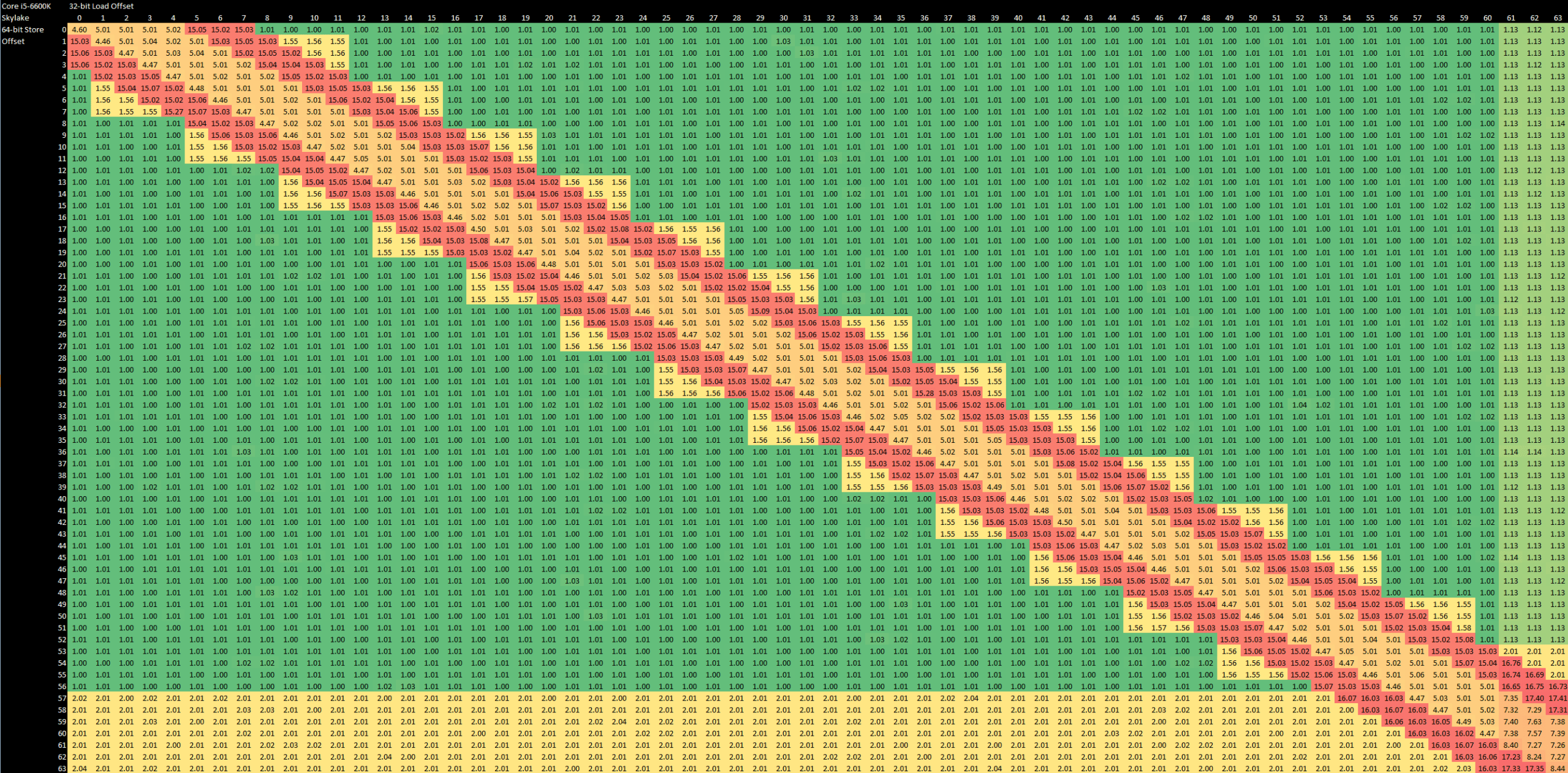
Goldmont Plus certainly does this and can only do fast forwarding for exact address matches, with a latency of 5 cycles. Other forwarding cases fail even if the store is contained within a younger load, and even the address match case fails if the load crosses a 64B cacheline boundary. Memory dependencies not handled by the fast case incur a 10-11 cycle penalty.
Non-overlapping accesses can still incur that 10-11 cycle penalty if they’re too close together. The jagged edge in the diagram above makes it feel like Goldmont Plus is adding the store address to the store width, and decides whether to block a subsequent load without comparing the two lowest address bits. To be fair, Sandy Bridge, Haswell and Skylake show a similar pattern, but can quickly detect a false dependency and recover without taking the full penalty.
Skylake can also forward data to any load contained within a store, and can do that across 64B cacheline boundaries with little penalty. Loads that cross a cacheline also incur little penalty on Skylake because there’s enough L1D bandwidth to handle two loads and a store in a single cycle.
Address Translation
Operating systems rely on virtual memory, which gives each process its own virtualized address space and prevents misbehaving programs from taking down the whole system. Virtual addresses are translated on-the-fly to physical ones, which can cause performance loss if the CPU has to make additional memory accesses to look up the translation. Therefore, CPUs cache frequently used translations in structures called TLBs to speed this up.

Goldmont Plus has a 32 entry dTLB, able to cover 128 KB with 4K pages. Then, a 512 entry L2 TLB helps handle programs with larger memory footprints. This L2 TLB can handle both instruction and data translations, an improvement over Goldmont where it only covered data-side translations. However, capacity is still meager compared to higher performance designs. AMD’s Zen architecture has larger first level TLBs, and has several times as much L2 TLB coverage.
I don’t have a way to measure instruction side TLB latency, but on the data side, hitting the L2 TLB adds eight extra cycles of latency. Eight cycles is comparable to Skylake’s 9 cycles of L2 TLB latency, or AMD Zen 2’s 7 cycles. However, that latency hurts more on Goldmont Plus because of low clock speeds.
Cache and Memory Access
Caching is important for any CPU because of high DRAM latency. Goldmont Plus uses a two-level cache hierarchy. A shared L2 serves as a last level cache, making it similar to Cortex A72 clusters or Intel’s older Core 2. GLP’s data-side memory hierarchy starts with a 24 KB L1 data cache. It’s a step down from the 32 KB L1D caches typically found in Intel or AMD’s higher performance cores.

L2 has 19 cycle latency, which isn’t bad for a multi-megabyte shared cache. It’s slightly faster than Cortex A72’s L2 cache in a similar configuration. It also offers better latency than Skylake’s L3 cache even when the latter’s higher clock speeds are accounted for. However, Skylake has a fast mid-level cache that insulates cores from last level cache latency.

Intel’s older Core 2 is another interesting comparison, because it’s a high performance core with a two-level cache. Core 2’s L2 serves the function of Skylake’s L2 and L3. It’s big enough to act as a last level cache, yet has low enough latency to act as a first stop for L1D misses.

Core 2 is likely able to achieve this by not sharing one L2 instance across four cores. Intel’s Core 2 Quad actually consists of two dual core clusters, each with its own L2. It’s not as efficient with die area because the two clusters together have 8 MB of cache, but a single core can only use 4 MB. Goldmont Plus in contrast still focuses on area efficiency. A single 4 MB cache takes far less area than two and avoids caching the same data twice, while still giving a single core the same last level cache capacity.
Despite having a modern integrated memory controller, the Celeron J4125 suffers over 180 ns of DRAM access latency at a 1 GB test size. Core 2 has just 68.86 ns of DRAM latency at the same test size with an antiquated FSB setup. Unlike with Meteor Lake, Goldmont Plus’ memory latency doesn’t significantly change if I load another core with a memory bandwidth test. Therefore, high memory latency can’t be explained by the memory controller failing to exit a low power mode.
Bandwidth
Memory bandwidth can be important, especially with multithreaded, vectorized workloads. The Celeron J4125 has four cores like many Intel client CPUs of that period. But unlike Intel’s higher performance cores, Celeron J4125 has lightweight vector units, no SMT, smaller out-of-order buffers that limit its ability to extract memory level parallelism, and runs all that at low clock speeds. That makes it demand far less bandwidth than say, Intel’s Core i7-7700K.

Goldmont Plus can load 16 bytes per cycle from its L1 data cache using SSE vector accesses. L2 bandwidth is around 8 bytes per cycle. It’s a lot like Intel’s Core 2 from a decade ago, but falls far behind Skylake. Skylake is optimized for vector workloads, and can perform two 32 byte loads per cycle at much higher clock speeds. A single Skylake core can actually sustain higher bandwidth from L3 than Goldmont Plus can from L1.
Write bandwidth tells a similar story, though Skylake has less of an advantage because its data cache only has one write port. Still, Skylake’s high clock speeds and 256-bit vector accesses let it hit pretty hard.

Goldmont Plus again handles like Core 2, but has much lower DRAM write bandwidth from a single core. L1D write bandwidth is also suspicious, with a strange drop off after 4 KB.
Write-Through L1D?
That drop-off reminds me of AMD’s Bulldozer and Piledriver architectures, which use a write-through L1D with a 4 KB write-coalescing cache. Performance counters seem to confirm that. Testing writes with an array larger than 4 KB causes write accesses to the 4 MB last level cache.

This design isn’t as bad as Pentium 4’s pure write-through L1D. As with Bulldozer and Piledriver, Goldmont Plus probably has 4 KB of write-back storage that can insulate the L2 cache from write traffic. Not having a full write-back L1D will cause additional L2 write traffic, which isn’t great when the L2 already handles more read traffic thanks to Goldmont Plus’ smaller 24 KB L1D.
L2 and DRAM
Thankfully Goldmont Plus’ L2 bandwidth scales well. It’s impressively close to Core 2 Quad’s L2 bandwidth, even though Core 2 Quad has two separate L2 cache instances. Goldmont Plus’ L2 bandwidth is also well ahead of Cortex A72‘s, which tops out at just under 37 GB/s. However, it’s far off from Skylake’s high performance L3, which uses a scalable ring bus and distributed cache controllers.

DRAM bandwidth on the Celeron J4125 is substandard. It should have a dual channel DDR4-2400 configuration just like the Core i7-7700K, but achieves around half as much read bandwidth. As a consolation prize, the Celeron does beat the old Core 2 by a substantial margin. Core 2 and Goldmont Plus might have similar bandwidth and reordering capacity, but Goldmont Plus benefits from a modern integrated memory controller.
Core to Core Latency
This test measures how fast we can bounce a cacheline between two cores with locked compare and exchange operations. The Celeron J4125 offers consistent latency between cores since they’re all in the same cluster, but latency is consistently high. Intel’s higher performance cores like Skylake perform better. I doubt this has anything to do with interconnect speed, because bandwidth is not an issue and Goldmont Plus’ shared L2 has comparable latency to Skylake’s shared L3. Rather, Skylake cores are probably better optimized for dealing with contended locks.

Final Words
Balancing a modern CPU core is a complex task. If an out-of-order execution engine is too small, its buffers will often fill and the core will struggle to find instruction level parallelism. But as buffer sizes get larger, they run into diminishing returns. Their full capacity might be rarely utilized. And when they do fill, the increased size might bring limited benefits. No sanely sized reorder buffer can avoid stalling when faced with DRAM latency for example.
With that in mind, I like Goldmont Plus. It has large enough register files, queues, and schedulers to make out-of-order execution shine, unlike Silvermont. GLP also compares well to low power cores like Cortex A72, with a better L2 cache and branch prediction. Compared to high performance desktop CPUs, GLP avoids chasing diminishing returns. Everything is done in moderation, while avoiding area and power hungry features like wide vector execution.
As for keeping the core balanced, most of Goldmont Plus’ tradeoffs make sense for a low power design, but it still has a pile of weaknesses. DRAM performance is poor. The 24 KB L1 data cache should be bigger and needs to be fully write-back. AMD’s Jaguar supported AVX by splitting 256-bit vectors into two 128-bit halves, and Goldmont Plus could really use that capability. At the frontend, GLP suffers from slow branch handling. Intel would rectify these issues in Tremont, likely leaning on the improved 10nm process node to do so.
But the biggest tradeoff comes from targeting higher performance than early Atoms. Larger buffers and schedulers consume more power, and all-core workloads can easily push package power above 13W. It’s going to throttle heavily in a fanless tablet or cell phone. But add even a tiny fan, and a 2c/4t Skylake ULV chip can offer much better single threaded performance. Maybe that’s why Goldmont Plus, and Goldmont before it, feel like forgotten Atom generations. It’s a pity because Goldmont Plus feels like a better balanced core than early Atoms, and should compete well against other low power CPUs like AMD’s Jaguar.
Therefore, Goldmont Plus is a snapshot of Intel’s Atom line progressing through an awkward transitional phase. We see the quad-core clusters that characterize subsequent Atom generations. The cluster interfaces with the rest of the system using the IDI protocol, so it already speaks the same language as ring bus (or mesh) agents in higher performance Intel designs. But Atom at this point isn’t ready to step into a hybrid design yet, and Intel’s 14 nm node isn’t good enough to let a balanced out-of-order core shine at low power levels.
If you like our articles and journalism, and you want to support us in our endeavors, then consider heading over to our Patreon or our PayPal if you want to toss a few bucks our way. If you would like to talk with the Chips and Cheese staff and the people behind the scenes, then consider joining our Discord.