


Can China’s Loongson Catch Western Designs? Probably Not.

We previously looked at Loongson’s 3A5000 and 3A6000. The LA464 and LA664 cores in those chips are the most promising Chinese domestic designs we’ve seen so far. Both are capable of reasonable performance per clock, though absolute performance is still several generations behind current Intel and AMD CPUs because of their low clock speeds. I’ve seen comments suggesting China is on course to match western companies like AMD and Intel. Predicting the future is always difficult, but history often repeats. With that in mind, I think it’s good to look at Loongson’s history.
Loongson grew out of a Chinese state sponsored effort to develop domestic CPUs. China’s 10th Five-Year Plan funded CPU development via the 863 and 973 projects4. That CPU development took place in the Institute of Computing Technology (ICT) at the Chinese Academy of Sciences. The resulting Godson-1 CPU was a 32-bit, 2-wide out-of-order core and 16 KB L1D/L1i caches. It ran at 266 MHz on a 130 nm CMOS process. I wasn’t able to find the paper on that CPU, so I’ll move on to Godson 2.
Godson-2: Setting the Baseline
ICT developed Godson-2 around 2003. Godson-2 is a 64-bit, 4-wide out-of-order core running at 434 MHz, and occupied 41.54 mm2 on a SMIC 180 nm process. It’s a massive upgrade over Godson-1, with a large clock speed increase accompanied by higher performance per clock.

In 2003, AMD served mobile, desktop, and server applications with their K8 architecture. K8 is a 3-wide out-of-order architecture that uses the x86-64 instruction set. On the 130 nm SOI process, K8 runs slightly above 2 GHz and occupies 193 mm2. The Athlon 64 FX-51 for example runs at 2.2 GHz.

Godson-2 has a wider pipeline, but K8 has a much larger out-of-order execution engine and would be better at absorbing latency. K8 possibly has a performance per clock advantage, but I suspect it’s not a huge one. But even if Godson-2 has competitive performance per clock, K8 clock so much higher that Godson-2 can’t hope to provide competitive performance.

Deeper in the core, ICT managed to implement state-of-the-art features in the pipeline. The branch predictor has a two-level prediction scheme typical for the time. The out-of-order engine uses an advanced PRF-based execution scheme that minimizes data movement. But all of Godson’s registers are only 64 bits wide, so data movement wasn’t heavy in the first place. PRF-based schemes would be more advantageous when CPUs moved to 256-bit or 512-bit vector registers. Still, ICT’s engineers were reasonably up to date with the latest architecture techniques.
Even though Godson-2 had a modern out-of-order execution setup, its system level architecture was dated. It used an off-die L2 cache at a time when both Intel and AMD had transitioned to full speed on-die L2 caches. Applications with large memory footprints would be further impacted by Godson-2’s lack of a L2 TLB.
Thoughts on Godson-2
Godson-2 is an interesting take at a low power CPU. It apparently consumed 2-3 W when running at 400 MHz, putting it in a lower power segment than AMD and Intel’s contemporary chips. Making a lower performance, lower power chip is an easier task than pushing the boundaries of high performance, but Godson-2’s designers did a pretty competent job with sensible tradeoffs.
More importantly, ICT’s engineers demonstrated they could develop a wide, out-of-order design. They also weren’t living under a rock, and were well aware of Godson-2’s weaknesses.
Improvements on the instruction fetch system include more precise branch prediction and support for SMT (Simultaneous Multi-threading). Improvements on memory system include on-chip level-two cache implementation, cache coherence for SMP and on-chip DDR memory interface
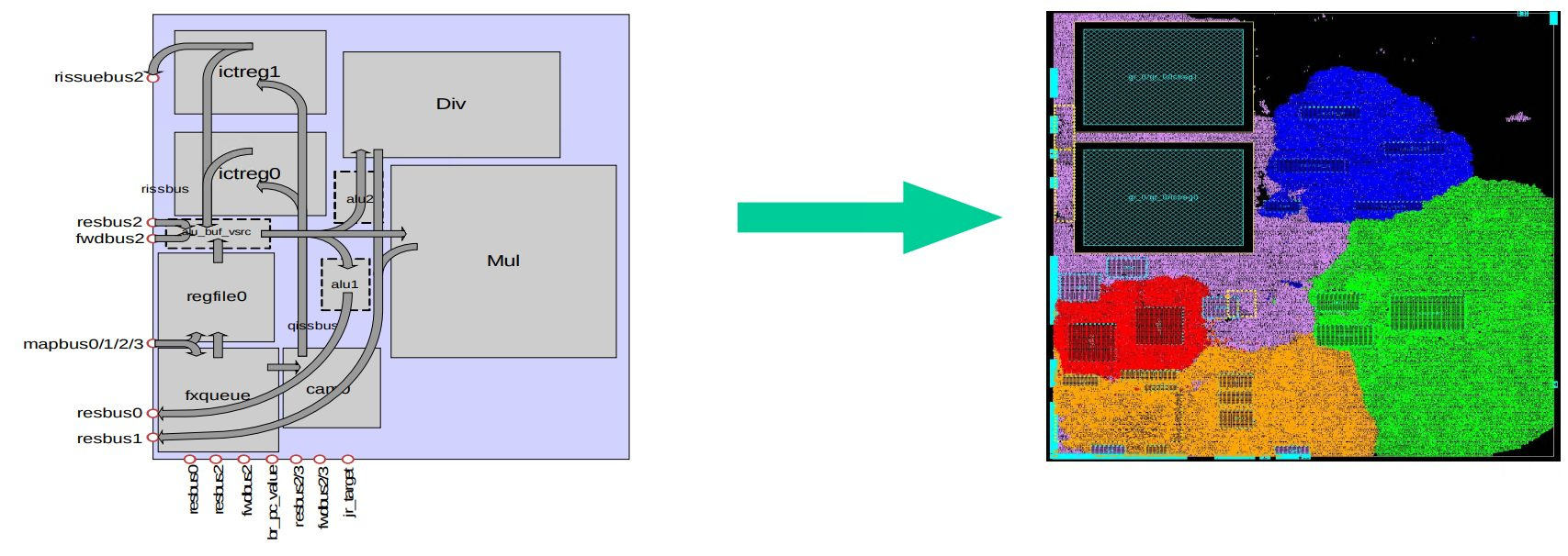
Microarchitecture of the Godson-2 Processor
Their focus on SMP (multi-socket) and creating an integrated memory controller showed they were closely watching AMD’s progress in those areas. They were also aware of state-of-the-art technologies being used at Intel, as they evaluated implementing SMT.
Godson-2E: Going a Bit Bigger
Godson-2E in 2006 tries to address Godson-2’s low clock speed and resulting low performance. It was funded by the 11th Five Year Plan, which aimed to optimize the chips created in the previous Five Year Plan.

Godson-2E is implemented with 47 million transistors on STMicroelectronics’s 7-metal, 90 nm CMOS process, and occupies 36 mm2. Clock speed increased to 1 GHz, and power consumption went up to 5-7 W. Godson-2E therefore aims higher than Godson-2, which drew 2-3 W at 400 MHz.

Around 2006, AMD kept using the same K8 design. But improved process nodes allowed higher clock speeds and dual core dies. In the same year, Intel came back from their mediocre Pentium 4 architecture in dramatic fashion. Core 2 did away with Pentium 4’s inefficiencies with a dramatically scaled up version of Intel’s P6 architecture.

For Godson-2E, ICT expended significant effort to increase clock speed. They moved to a 9 stage pipeline, compared to the 7 stage one used by Godson-2. They redesigned the integer register file by creating two copies of it to reduce port count.
Replicating the register file may seem wasteful, but it’s a common technique to trade area for higher clocks. AMD’s Bulldozer does the same thing.

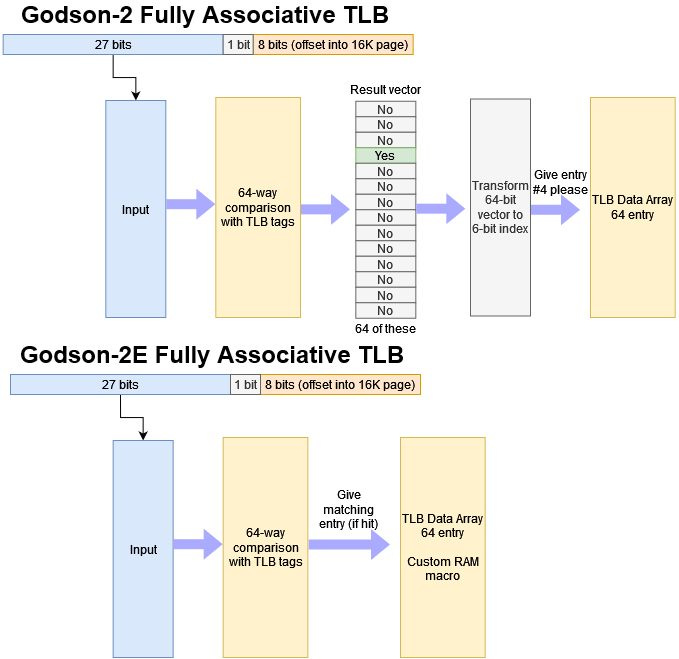
ICT’s engineers went further because clock speed is limited by the slowest part of the core. They optimized the TLBs with custom RAM macros, letting them remove unnecessary steps.
IPC Improvements
Besides improving clock speed, ICT went after performance-per-clock increases by increasing the ROB size and modernizing the memory subsystem. Godson-2E gets a 512 KB, 4-way L2 with 9 cycle latency, and an on-chip memory controller. However, Godson-2E still could not match AMD’s cache and memory performance. The contemporary 2.8 GHz Athlon FX-62 had 4.6 ns of L2 latency compared to Godson-2E’s 9 ns. Both cores can pull 4 bytes per cycle from L2, so Athlon FX-62 has 11 GB/s of bandwidth to Godson-2E’s 4 GB/s.

Godson-2E’s memory controller was also a disappointment with about 1 GB/s of bandwidth.

AMD’s Athlon FX-62 has about four times as much memory bandwidth.

To ICT’s credit, their engineers are undoubtedly doing their best to keep up with modern features like integrated memory controllers and on-die L2 caches, even if the implementation result falls a bit short.
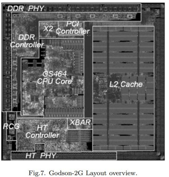
Godson-2G: Binary Translation
Godson-2G takes the basic GS464 core from Godson-2E and moves to STMicroelectronics’s 65 nm CMOS process. Performance per clock should improve slightly thanks to a DDR2/3 memory controller and a bigger 1 MB L2, but the core didn’t see higher clocks or architecture improvements. Die area increased to 53.54 mm2, likely because of the larger L2 cache.
Instead of focusing on core performance, ICT worked on binary translation. A CPU is only as useful as the programs it can run, and MIPS64 was not a good place to be. ICT therefore tried to reduce binary translation overhead to make running x86 software more practical. They added instructions to handle x86 flags.

On the floating point side, they added new 2×64 load/store instructions, letting them emulate an x86 FLD+FMUL+FSTP sequence with just eight instructions. Godson’s decoder got additional logic to track the x87 top of stack pointer too. Then, ICT figured out how to implement L1D/L1i coherency, reducing expensive instruction cache flushes after the binary translator does its job. While not mentioned in the ICT’s paper, instruction cache coherency should improve performance in other code load scenarios too.
Software Ecosystem Comments
Making a competitive CPU is difficult enough. But on top of that, ICT has to invest significant effort in bringing the software ecosystem up to speed. That’s probably why the core saw minimal changes for a while.
Apple had the same challenge when transitioning to their in-house 64-bit ARM cores. Today, other 64-bit ARM cores are similarly tackling the compatibility problem via binary translation.
Godson-3: Multi-Core Time
Single core CPUs were on their way out by the mid to late 2000s, so Godson 3 places four GS464 cores on a 8×8 AXI crossbar and connects that to a shared 4 MB L2 cache. It taped out on STMicroelectronics’s 65nm process in 2008, and occupied 173.8 mm2. Clock speed remained at 1 GHz, and power consumption remained low at 5-10W. ICT also used the AXI crossbar to attach HyperTransport controllers, letting Godson 3 scale to higher core counts with multi-die configurations.

In 2008, Intel’s Nehalem architecture similarly implemented four cores on a monolithic die. A central “Global Queue” acted as a crossbar between four cores and a shared 8 MB L3 cache. Unlike Godson 3, Nehalem used 256 KB mid-level caches to insulate cores from L3 latency, creating a triple level cache hierarchy that continues to be used in CPUs today. Intel’s new QPI interconnect gave them an equivalent to AMD’s HyperTransport, and let Nehalem efficiently scale in multi-socket setups.

AMD used similar techniques to make quad core CPUs. Four K10 cores were connected to 2 MB of L3 cache through a crossbar. However, AMD had trouble and clock speeds regressed to around 2.6 GHz, down from K8’s 3 GHz+ clocks on similar nodes.
Godson-3B and GS464V
Godson-3B was described in an ISSCC 2011 paper. At this point, authors in the paper start to be affiliated with both the Chinese Academy of Sciences and Loongson Technologies, so I’ll switch over to saying Loongson.

Godson-3B focuses on floating point throughput and gets 256-bit vector support. Intel’s Sandy Bridge also launched with 256-bit vector support in 2011, but GS464V actually one-ups Sandy Bridge because it supports fused multiply-add (FMA), letting it achieve more per-cycle floating point throughput.
However, Sandy Bridge can clock more than twice as high, completely negating GS464V’s advantage. Beyond vector execution, Sandy Bridge has a substantially larger out-of-order execution engine. Its reorder buffer has more than twice as many entries, and its unified scheduler has more entries than GS464V’s FP/vector and integer schedulers combined. Loongson’s paper doesn’t note any other core changes, so I assume everything else remains the same compared to GS464.
System Level
On the core count front, Loongson managed to create an octa-core chip by linking two quad core clusters. The resulting Godson-3B chip has 4 MB of L2 (probably 2 MB per cluster) and uses a 299.8 mm2 die. A dual channel DDR2 or DDR3 setup can provide 12.8 GB/s or 25.6 GB/s of memory bandwidth, respectively.

For comparison, Intel created octa-core Nehalem parts and 10 core Westmere parts with scalable ring interconnect. All cores on the die can share a massive 24 MB L3 cache, and anything that misses in L3 can be served by a quad-channel DDR3 setup.

Godson-3B’s large vector units do give it a remarkable 256 GFLOPS of FP32 throughput compared to Nehalem-EX’s 145.28 GFLOPS at 2.27 GHz, while also consuming less die area and power. However, Godson-3B’s limited memory bandwidth and low cache capacity would make it harder to feed.
Godson-3B1500: Cache Hierarchy Changes
Godson-3B1500, detailed in an ISSCC 2013 paper9, migrates the 8 core GS464V setup to STMicroelectronics’s 32nm node. Last level cache capacity increases to 8 MB (probably two 4 MB clusters), and 128 KB mid-level caches get added to insulate cores from L3 latency. Thanks to the improved process nodes, Loongson was able to increase clock speed to 1.2 GHz at 1.1V, or 1.5 GHz at 1.3V. 1.5 GHz is still a very low clock speed, but it represents a 50% increase from the Godson-3B’s 1 GHz. Loongson ported the 3B1500 to STMicroelectronics’s 28 nm node, which reduced die size from 182.5 mm2 to 140.8 mm2.

Loongson also published latency data for the 3B1500’s cache hierarchy, suggesting that the 128 KB L2 cache has approximately 19 cycles of latency. For comparison, Intel’s Haswell architecture had 12 cycle L2 latency, and had twice as much L2 capacity.

The 3B1500’s L3 cache is not tied to the core clock, and runs at 1 to 1.1 GHz. Haswell similarly has decoupled L3 cache clocks, but can run its “uncore” much faster. 3B1500 has similar L3 latency (in clock cycles) to octa-core Haswell, and can get to DRAM in fewer cycles because it clocks so much lower.

Overall, the 3B1500 is a stronger octa-core chip than the Godson 3B. But its mid-level cache appears to have mediocre performance, and it still suffers from the low memory bandwidth of its predecessor. Although 3B1500 enjoys a significant clock speed increase, it’s still clocked too low to compete with contemporary western designs.
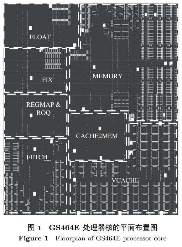
GS464E: Core Catch Up Time
Toward the mid 2010s, Loongson’s CPU architecture basically stood still as engineers focused on software or core scalability. GS464 started its life offering decent performance per clock, even though it couldn’t run at the clock speeds necessary to be competitive against Intel and AMD designs. But in 2013, GS464 was far behind even from the performance per clock perspective. GS464E tries to catch up.
Loongson’s engineers researched IBM’s Power7, Intel’s Ivy Bridge, and Arm’s Cortex A9. Evidently they concluded everything in GS464 had to get bigger. The reorder buffer, schedulers, branch ordering queue, and memory access queue all received significant capacity increases. Address translation performance benefited from a large 1024 entry L2 TLB. An extra address generation unit lets GS464E complete two memory accesses per cycle, which represents a significant upgrade from GS464’s single AGU pipe.

Other execution units were left largely unchanged. GS464V’s 256-bit vector capability was not carried forward, likely because it took too much power and area. To summarize some other changes:

The GS464E architecture ends up being far more capable than its predecessor. GS464E is a significant step behind the likes of Sandy Bridge and Haswell, but Loongson has at least made the gap smaller.
But GS464E had huge problems if we look beyond per clock performance. The quad core 3A1500 chip consumes 248.6 mm2 of die area on a 40 nm CMOS node of unspecified origin. For comparison, Loongson’s prior 8 core 3B1500 chip only took 182.5 mm2 on STMicroelectronics’s 32nm node. 3B1500 clocked higher too. Maybe Loongson’s engineers struggled to keep clock speed up with larger core structures. But Loongson ten years ago was able to more than double clock speed while using techniques like replicated register files to increase clock speed. And Loongson’s 3B1500 had large 256-bit vector units fed by a relatively large 28 entry scheduler, which GS464E cuts back on.
Process node is another culprit. The 40nm node may be a Chinese domestic one, and likely wasn’t as good as STMicroelectronics’s nodes. Loongson’s paper10 noted that GS464E enjoyed a 54.9% score advantage in SPEC CPU 2000’s integer benchmarks compared to the 1 GHz Loongson 3A, a quad core GS464 implementation on 65nm CMOS. Dropping from 1.5 GHz to 1 GHz would erase most of that score improvement.
LA464 and LA664
LA464 switched to SMIC’s 12 nm process, and brought clock speeds up to 2.5 GHz. It also increased scheduler capacity, added two more ALU ports, and implemented larger load/store queues. We have a full article on that here, so I’ll keep things short.
We saw LA464 provide decent performance per clock, though 2.5 GHz is still too low to compete. LA664 further improves performance per clock with a large architectural upgrade. Again, see our separate article for more details.
Clock Speeds
Loongson managed an impressive performance per clock increase from 3A5000 to 3A6000. But drawing a line between those two points paints an unrealistically rosy picture. Loongson was arguably on an even better trajectory in 2006, when Godson-2 massively increased IPC and Godson-2E more than doubled clock speed after that. But Godson-2E couldn’t get close to contemporary AMD/Intel CPUs because of its low clock speed. Loongson’s 3A6000 suffers from the same problem today.
Performance at the same clock is not a good microarchitectural goal, if it means building bottlenecks into the pipeline that will forever impact clock frequency…
It is equally meaningless to brag about high clock frequency without considering CPI and other significant performance trade-offs made to achieve it.David B. Papworth, Tuning the Pentium Pro Microarchitecture
Good CPU design involves getting a balance of clock speed and performance per clock that maximizes performance. Loongson and ICT have consistently done well on the performance per clock front but not clock speed. It’s certainly possible to get competitive performance via emphasizing performance per clock. Apple is well known for this. Their cores use more reordering capacity, wider core width, and large L1 caches to get higher performance per clock than contemporary Intel/AMD designs. But even then, Apple needs clock speeds above 3 GHz to get good performance. Loongson doesn’t have the advantages Apple’s core has, and clocks lower.
Core Count
Today’s applications are more multithreaded than those of the early 2000s, so higher core count can significantly improve performance. Loongson somewhat kept up in the early 2010s, but today their system architecture is far behind. The 3A6000 is a quad core chip in 2024, when octa core chips are widely affordable. AMD’s 7700X for example sells for the price of a domestic flight ticket (just above $300). Higher end chips like the 7950X and Intel’s 14900K can offer previously server grade multithreaded performance at consumer price points. Loongson’s quad core chips are woefully out of place in such an environment.
Increasing core count isn’t straightforward either, because it requires a flexible interconnect. Loongson previously used HyperTransport to reach higher core counts. But HyperTransport is a technology that was at its prime before 2010, and using it to link core clusters results in NUMA (Non-Uniform Memory Access) configurations. Optimizing software for NUMA is a lot harder, and many consumer applications aren’t NUMA aware. AMD and Intel can create 16 core UMA setups, which make it easier for performance to scale with core count.
Software
CPUs are only as useful as the programs they can run. Loongson managed to make a mess out of the situation at several levels. At the OS level, Loongson’s CPUs have two binary-incompatible Linux distributions. At the application level, Loongson faces software optimization problems. Developers will optimize programs for the most common CPUs like x86 and ARM ones. Web browsers are one example. Loongson ships LBrowser v3, a Chromium based browser. It performs horribly on the Speedometer 3.0 browser benchmark:

For comparison, AMD’s Ryzen 3950X scores 15.9 when running Speedometer 3.0 under Google Chrome. Zen 2 only had a 40% performance advantage when both chips enjoyed hand-optimized assembly in libx264. With this browser benchmark, it’s a 483% difference in favor of AMD’s now four year old CPU.
Things could get even worse if Loongson has to use binary translation to run a wide range of programs compiled for x86. Losing performance to binary translation might be okay if your baseline performance is reasonably competitive (as in Apple’s case). Loongson is already far behind when running native code.
Final Words
Loongson represents China’s most promising domestic CPU development effort. Yet comments suggesting it can compete with the best western designs feel a bit off. Loongson has always been okay at achieving decent performance per clock, but never had a balanced design with high enough clock speeds to deliver competitive final performance. Their most recent 3A5000 and 3A6000 CPUs merely continue that trend. Furthermore, Loongson’s traditional software ecosystem problems remain. Their core count deficit is even more severe now than it was 10 years ago.
Better process nodes can help with the clock speed and core count problems. But Loongson doesn’t have good prospects there either because they have to make completely domestic designs. Even US chip designers like AMD don’t use domestic nodes. AMD’s Zen 4 uses TSMC’s 5 nm process. Intel has domestic fabrication plants, but even they are dipping into TSMC nodes from time to time. That’s because globalization lets countries focus their resources on getting really good in a certain area, rather than splitting them and doing a mediocre job across a wider variety of fields. Loongson doesn’t get to enjoy the benefits of globalization and specialization. Even if Loongson gets enough funding to attract engineering talent like Apple, Intel, or AMD, they’ll still be handcuffed by their goal of producing domestic designs.
If you like our articles and journalism, and you want to support us in our endeavors, then consider heading over to our Patreon or our PayPal if you want to toss a few bucks our way. If you would like to talk with the Chips and Cheese staff and the people behind the scenes, then consider joining our Discord.
References
Wei-Wu Hu, Fu-Xin Zhang, and Zu-Song Li, Microarchitecture of the Godson-2 Processor
Wei-Wu Hu, The Godson-3 Multi-Core Processor and its Application in High Performance Computers
Wei-Wu Hu, Ji-Ye Zhao, Shi-Qiang Zhong, Xu Yang, Ellio Guidetti, and Chris Wu, Implementing a 1 GHz Four-Issue Out-of-Order Execution Microprocessor in a Standard Cell ASIC Methodology
Wei-Wu Hu, Yifu Zhang, Jie Fu, Introduction to CPU and DSP design in China
Ji-Ye Zhao, Dong Liu, Dan-Dan Huan, Meng-Hao Su, Bin Xiao, Ying Xu, Feng Shi, Chen Chen, and Song Wang, Physical Design Methodology for Godson-2G Microprocessor
Milena Milenkovic, Aleksandar Milenkovic, Jeffrey Kulick, Demystifying Intel Branch Predictors
Wei-Wu Hu, Jian Wang, Xiang Gao, Yunji Chen, Qi Liu, and Guojie Li, Godson-3: A Scalable Multicore RISC Processor with x86 Emulation
Wei-Wu Hu, Ru Wang, Yunji Chen, Baoxia Fan, Shiqiang Zhong, Xiang Gao, Zhichu Qi, and Xu Yang, Godson-3B: A 1 GHz 40W 8-Core 128 GFLOPS Processor in 65nm CMOS
Weiwu Hu et al, Godson-3B1500: A 32nm 1.35GHz 40W 172.8 GFLOPS 8-Core Processor
吴瑞阳, 汪文祥, 王焕东, 胡伟武, 龙芯 GS464E 处理器核架构设计